
Nanocontact Printing and AFM Nanolithography
The atomic force microscope as a mechano-electrochemical pen
Christian Obermair, Andreas Wagner and Thomas Schimmel
Beilstein Journal of Nanotechnology 2011, 21 659-664
Abstract
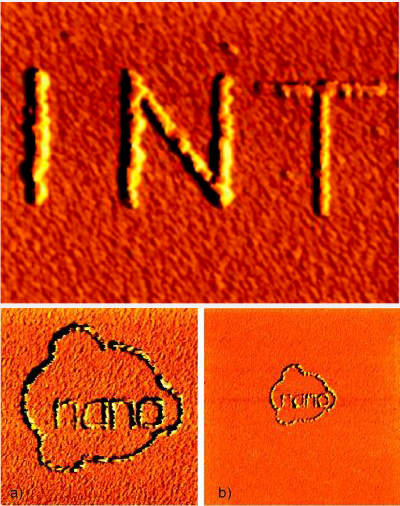 We demonstrate a method that allows the controlled writing of metallic patterns on the nanometer scale using the tip of an atomic force microscope (AFM) as a “mechano–electrochemical pen”. In contrast to previous experiments, no voltage is applied between the AFM tip and the sample surface. Instead, a passivated sample surface is activated locally due to lateral forces between the AFM tip and the sample surface. In this way, the area of tip–sample interaction is narrowly limited by the mechanical contact between tip and sample, and well-defined metallic patterns can be written reproducibly. Nanoscale structures and lines of copper were deposited, and the line widths ranged between 5 nm and 80 nm, depending on the deposition parameters. A procedure for the sequential writing of metallic nanostructures is introduced, based on the understanding of the passivation process. The mechanism of this mechano–electrochemical writing technique is investigated, and the processes of site-selective surface depassivation, deposition, dissolution and repassivation of electrochemically deposited nanoscale metallic islands are studied in detail.
Reversible mechano-electrochemical writting of metallic nanostructures with the tip of an atomic force microscope
Christian Obermair, Marina Kress, Andreas Wagner and Thomas Schimmel
Beilstein Journal of Nanotechnology 2012, 3, 824-830
Abstract
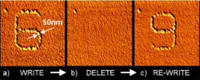 We recently introduced a method that allows the controlled deposition of nanoscale metallic patterns at defined locations using the tip of an atomic force microscope (AFM) as a “mechano-electrochemical pen”, locally activating a passivated substrate surface for site-selective electrochemical deposition. Here, we demonstrate the reversibility of this process and study the long-term stability of the resulting metallic structures. The remarkable stability for more than 1.5 years under ambient air without any observable changes can be attributed to self-passivation. After AFM-activated electrochemical deposition of copper nanostructures on a polycrystalline gold film and subsequent AFM imaging, the copper nanostructures could be dissolved by reversing the electrochemical potential. Subsequent AFM-tip-activated deposition of different copper nanostructures at the same location where the previous structures were deleted, shows that there is no observable memory effect, i.e., no effect of the previous writing process on the subsequent writing process. Thus, the four processes required for reversible information storage, “write”, “read”, “delete” and “re-write”, were successfully demonstrated on the nanometer scale.