
Printing Technologies for Integration of Electronic Devices and Sensors
-
Author:
T. T. Baby, G. C. Marques, F. Neuper, S. A. Singaraju, S. Garlapati, F. von Seggern, R. Kruk, S. Dasgupta, B. Sykora, B. Breitung, P. A. Sukkurji, U. Bog, R. Kumar, H. Fuchs, T. Reinheimer, M. Mikolajek, J. R. Binder, M. Hirtz, M. Ungerer, L. Koker, U. Gengenbach, N. Mishra, Patric G., M. Tahoori, J. Aghassi Hagmann, H. von Seggern, H. Hahn
-
Source:
Functional Nanostructures and Sensors for CBRN Defence and Environmental Safety and Security. NATO Science for Peace and Security Series C: Environmental Security. A. Sidorenko, H. Hahn (eds.) Springer Nature B.V. (2020) 1-34
- Date: 2020
-
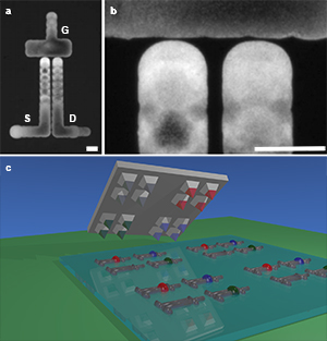
Many different methods, such as screen printing, gravure, flexography, inkjet etc., have been employed to print electronic devices. Depending on the type and performance of the devices, processing is done at low or high temperature using precursor- or particle-based inks. As a result of the processing details, devices can be fabricated on flexible or non-flexible substrates, depending on their temperature stability. Furthermore, in order to reduce the operating voltage, printed devices rely on high-capacitance electrolytes rather than on dielectrics. The printing resolu- tion and speed are two of the major challenging parameters for printed electronics. High-resolution printing produces small-size printed devices and high-integration densities with minimum materials consumption. However, most printing methods have resolutions between 20 and 50 μm. Printing resolutions close to 1 μm have also been achieved with optimized process conditions and better printing technology.