Nanomaterials for Electronic and Energy Applications
Welcome to the website of the Nanomaterials for Electronic and Energy Applications group! We research innovative and complex materials and develop their use for electronic and energy applications. To this end, we are developing novel materials, especially with a focus on functional nanomaterials and complex composites. Our science is divided into three research areas, which are closely related, High Entropy Materials, Functional Materials and Electronic and Energy Applications, more details about the topics and the respective work can be found in the corresponding subcategories linked below.
We work very closely with scientists from many other disciplines and look forward to any kind of cooperation. If you find our work exciting or are interested in a cooperation, please never hesitate to contact us!
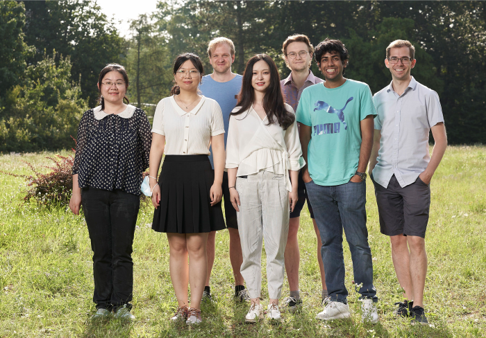
The team! The most important thing when it comes to good science.
Research
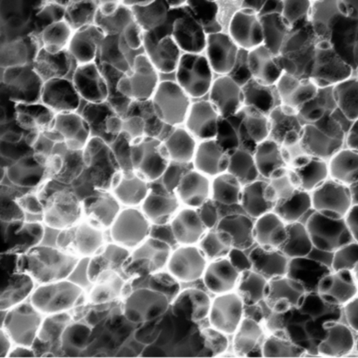
High Entropy Materials
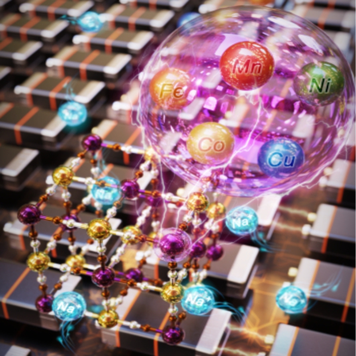
High entropy materials are a very innovative and complex class of materials based on the incorporation of many different elements into a single-phase crystal structure. The ability to tailor the properties of these materials by varying the stoichiometry, number and selection of elements makes them very interesting for a wide range of applications. We are utilizing the high-entropy approach for different structures and designing novel compounds.
Functional Materials
Functional materials are developed for a variety of applications. Porous, resistive, conducting and semiconducting, energy storage materials, and many more are prepared in our labs and later used for specific utilizations.
Electronic and Energy Applications
We use the developed materials for a great variety of different applications. Especially electronic and energy applications are in our focus of interest. Materials for printed devices, e.g. printed memristors or transistors, are prepared and implemented in printable functional inks for device preparation.