Equipment
For our research we are developing and using the following techniques:
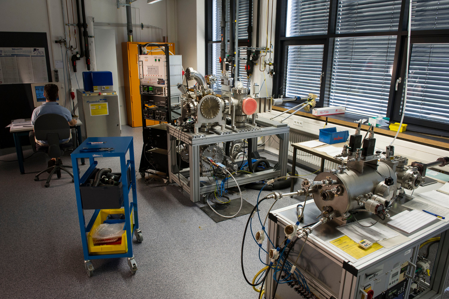
- Nanofabrication (multi-layer e-beam lithography, reactive ion etching, sputtering, atomic-layer deposition, packaging)
- Electric-field assisted deposition techniques (Dielectrophoresis)
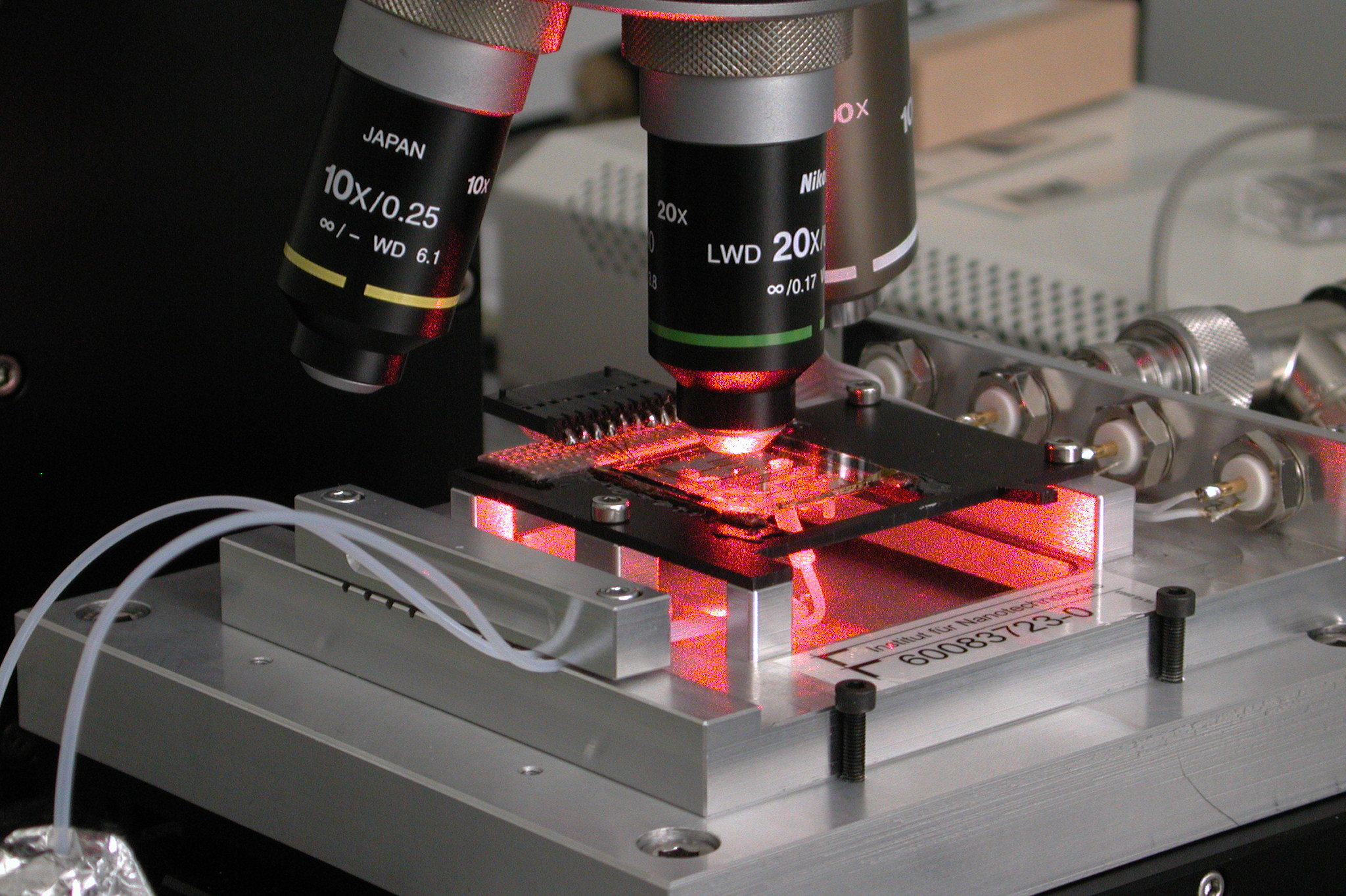
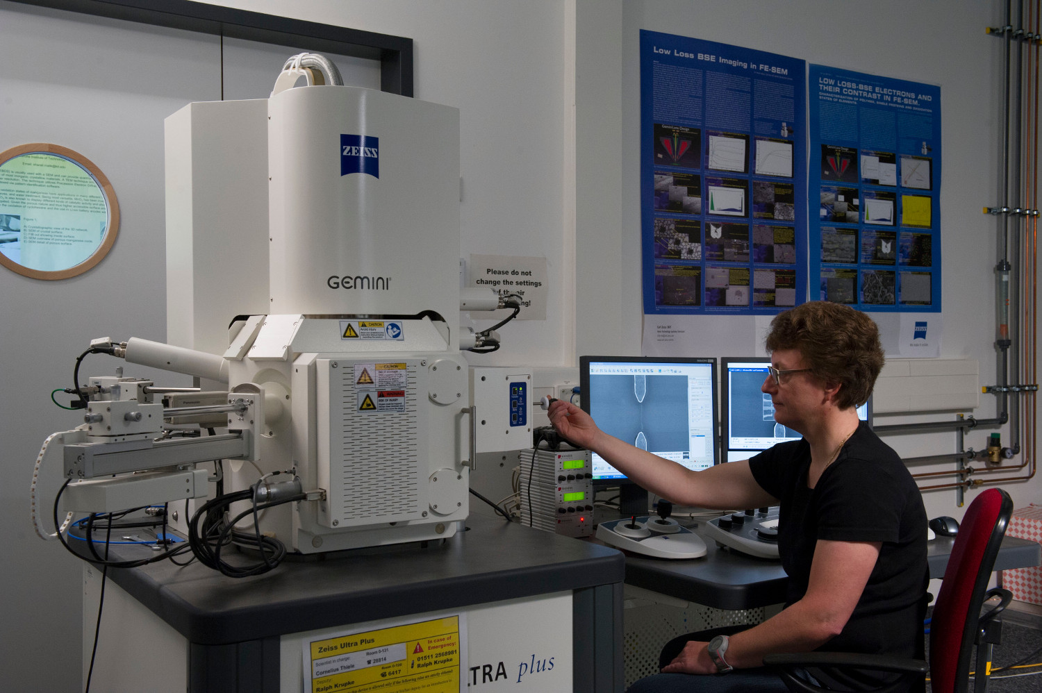
- Voltage-contrast scanning electron microscopy
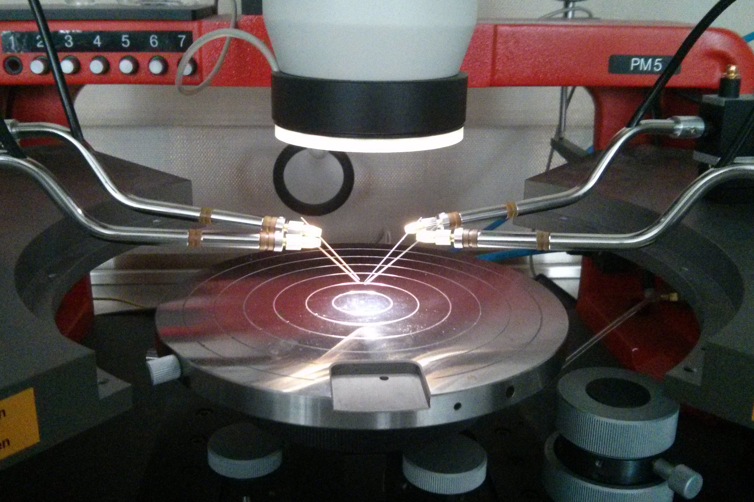
- Photocurrent spectroscopy and imaging
- Electroluminescence spectroscopy and imaging
- Raman spectroscopy and imaging
- Semiconductor parameter analysis and charge transport