
Organic Electronics
Amorphous organic semiconductors are used in many applications such as organic light emitting diodes (OLEDs) and organic photovoltaics (OPV). The almost unlimited variety of chemical compounds and material combinations makes experimental material and device improvement difficult.
The challenge in modeling charge transport in amorphous materials is twofold. Models must incorporate effects on vastly different length scales ranging from the electronic structure of single molecules in the sub-nanometer scale to percolation effects on distances up to the micrometer scale. Charge mobility and energy dissipation during transport depend exponentially on the energy disorder in amorphous systems, making accurate quantum mechanical analysis of large molecular systems necessary.
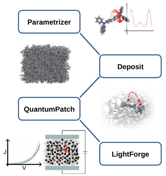
This challenge can be tackled using a multiscale approach for the simulation of charge transport in disordered organic materials. The methodology of this approach consists of several successive steps building upon one another. For the generation of atomistic morphologies, molecule specific force field parameters are required. These are determined using a quantum mechanical analysis of single molecules. The parameters obtained in this first step are then used in classical molecular dynamics or Monte Carlo methods for the generation of amorphous thin film morphologies. These systems are analyzed using quantum mechanical methods in order to extract electronic properties relevant for charge transport. In the last step, the master equation of charge transport in the amorphous system is solved using an analytical or numerical approaches such as kinetic Monte Carlo simulations.
Simulating the growth of amorphous organic thin films
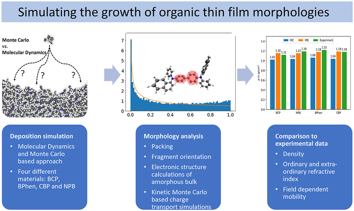
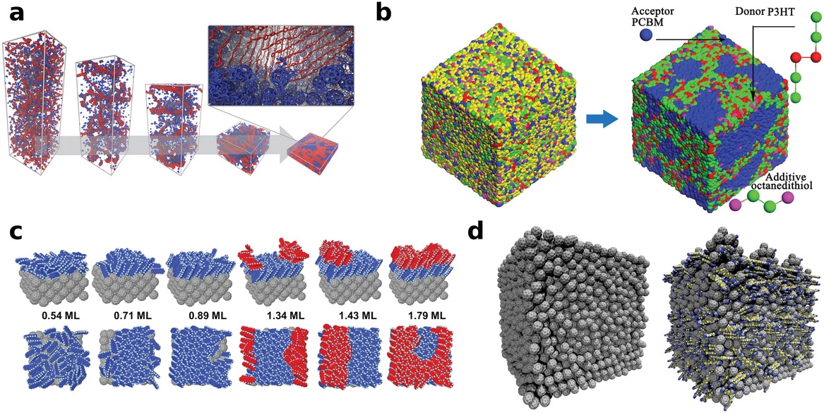
Physical vapor deposition is used widely to produce organic electronics devices, in particular for OLEDs and in recent years have seen a number of surprising observations, such as deposition-induced emitter orientation and built-in electrostatic potentials in thin organic films. In this paper, we compare two different modeling approaches, which both aim to simulate the physical vapor deposition (PVD) process for small organic molecules; A molecular dynamics approach, based on a classical bead-spring force field and time integration and a Metropolis Monte Carlo approach, where the intramolecular degrees are limited to the torsional rotations. To analyze the resulting structures, we calculate the density and radial distribution functions (RDF) of all films. We observe a good agreement for the RDFs, but an approximately 10% higher density for the films generated by the molecular dynamics approach. Additionally, we investigate the anisotropic nature of such morphologies by calculating the ordinary and extra-ordinary refractive index for each material. Finally, we calculate electron and hole mobilities with an Kinetic Monte Carlo protocol.
Systematic kMC Study of Doped Hole Injection Layers in Organic Electronics
Organic light emitting diodes (OLED) play an important role in commercial displays and are promising candidates for energy-efficient lighting applications. The performance of OLEDs is determined by a multifaceted interplay of materials and device architectures. The optimization of doped injection layers, to overcome the charge injection barrier from the electrodes to the organic layers, is critical for high-efficiency OLED devices, but has been driven mainly by chemical intuition and experimental experience. Therefore in this work, using a computer-aided method for material and device modeling, the parametric kinetic Monte Carlo model, we studied the effect of doped hole injection layers on the injection barrier in dependence on material and layer properties. We were able to quantitatively elucidate the influence of doping concentration, material properties, and layer thickness on the injection barrier and device conductivity, leading to the conclusion that our kMC model is suitable for virtual device design.
De Novo Calculation of the Charge Carrier Mobility in Amorphous Small Molecule Organic Semiconductors
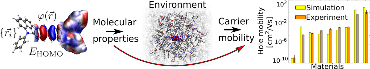
Organic semiconductors (OSC) are key components in applications such as organic photovoltaics, organic sensors, transistors and organic light emitting diodes (OLED). OSC devices, especially OLEDs, often consist of multiple layers comprising one or more species of organic molecules. The unique properties of each molecular species and their interaction determine charge transport in OSCs—a key factor for device performance. The small charge carrier mobility of OSCs compared to inorganic semiconductors remains a major limitation of OSC device performance. Virtual design can support experimental R&D towards accelerated R&D of OSC compounds with improved charge transport. Here we benchmark a de novo multiscale workflow to compute the charge carrier mobility solely on the basis of the molecular structure: We generate virtual models of OSC thin films with atomistic resolution, compute the electronic structure of molecules in the thin films using a quantum embedding procedure and simulate charge transport with kinetic Monte-Carlo protocol. We show that for 15 common amorphous OSC the computed zero-field and field-dependent mobility are in good agreement with experimental data, proving this approach to be an effective virtual design tool for OSC materials and devices.
De Novo Simulation of Charge Transport through Organic Single-Carrier Devices
In amorphous organic semiconductor devices, electrons and holes are transported through layers of small organic molecules or polymers. The overall performance of the device depends both on the material and the device configuration. Measuring a single device configuration requires a large effort of synthesizing the molecules and fabricating the device, rendering the search for promising materials in the vast molecular space both nontrivial and time-consuming. This effort could be greatly reduced by computing the device characteristics from the first principles. Here, we compute transport characteristics of unipolar single-layer devices of prototypical hole- and electron-transporting materials, N,N′-di(1-naphthyl)-N,N′-diphenyl-(1,1′-biphenyl)-4,4′-diamine (α-NPD) and 2,2′,2″-(1,3,5-benzinetriyl)-tris(1-phenyl-1-H-benzimidazole) (TPBi) using a first-principles multiscale approach that requires only the molecular constituents and the device geometry. This approach of generating a digital twin of the entire device can be extended to multilayer stacks and enables the computer design of materials and devices to facilitate systematic improvement of organic light-emitting diode (OLED) devices.
Computing Charging and Polarization Energies of Small Organic Molecules Embedded into Amorphous Materials with Quantum Accuracy
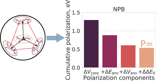
The ionization potential, electron affinity, and cation/anion polarization energies (IP, EA, P(+), P(−)) of organic molecules determine injection barriers, charge carriers balance, doping efficiency, and light outcoupling in organic electronics devices, such as organic light-emitting diodes (OLEDs). Computing IP and EA of isolated molecules is a common task for quantum chemistry methods. However, once molecules are embedded in an amorphous organic matrix, IP and EA values change, and accurate predictions become challenging. Here, we present a revised quantum embedding method [Friederich et al. J. Chem. Theory Comput. 2014, 10 (9), 3720−3725] that accurately predicts the dielectric permittivity and ionization potentials in three test materials, NPB, TCTA, and C60, and allows straightforward interpretation of their nature. The method paves the way toward reliable virtual screening of amorphous organic semiconductors with targeted IP/EA, polarization energies, and relative dielectric permittivity.
Analyzing Dynamical Disorder for Charge Transport in Organic Semiconductors via Machine Learning
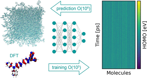
Organic semiconductors are indispensable for today’s display technologies in the form of organic light-emitting diodes (OLEDs) and further optoelectronic applications. To find or even design new organic semiconductors with higher charge carrier mobility, computational approaches, in particular multiscale models, are becoming increasingly important. Therefore, we overcome the problem of computationally very costly simulations due to the long timescale requirements, by integrating machine learning models into multiscale simulations. This allows us to obtain unprecedented insight into relevant microscopic materials properties, in particular static and dynamic disorder contributions for a series of application-relevant molecules. We find that static disorder and thus the distribution of shallow traps are highly asymmetrical for many materials, impacting widely considered Gaussian disorder models and furthermore analyze characteristic energy level fluctuation times and compare them to typical hopping rates to evaluate the importance of dynamic disorder for charge transport.
Disorder-driven doping activation in organic semiconductors
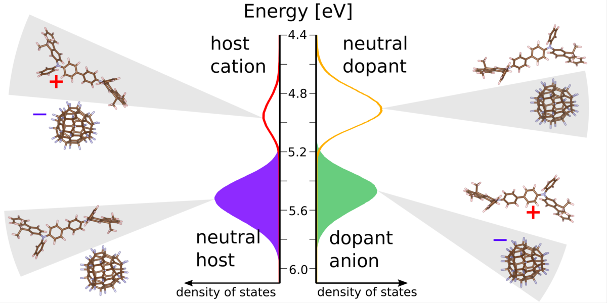
Conductivity doping of organic semiconductors is an essential prerequisite for many organic devices, but the specifics of dopant activation are still not well understood. Using many-body simulations that include Coulomb interactions and dopant ionization/de-ionization events explicitly we here show significant doping efficiency even before the electron affinity of the dopant exceeds the ionization potential of the organic matrix (p-doping), similar to organic salts. We explicitly demonstrate that the ionization of weak molecular dopants in organic semiconductors is a disorder-, rather than thermally induced process. Practical implications of this finding are a weak dependence of the ionized dopant fraction on the electron affinity of the dopant, and an enhanced ionization of the weak dopants upon increasing dopant molar fraction. As a result, strategies towards dopant optimization should aim for presently neglected goals, such as the binding energy in host-dopant charge-transfer states being responsible for the number of mobile charge carriers. Insights into reported effects are provided from the analysis of the density of states, where two novel features appear upon partial dopant ionization. The findings in this work can be used in the rational design of dopant molecules and devices.
Disorder compensation controls doping efficiency in organic semiconductors
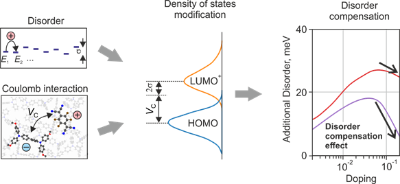
Doping in organic semiconductors is often described in terms of models inherited from the inorganic or “classical” theory, which neglects explicit contribution of strong Coulomb interactions and the localization of the charge carriers from organic counterparts.
Here, we consider the localization of the charge carriers and their mutual interactions in the realistic energetic landscape, using kinetic Monte Carlo (kMC) method. We show that strong Coulomb interactions of the ionized host-dopant pair (integer charge-transfer complex, ICTC) lead to the formation of the EA+ (polaron) levels, which are shifted with respect to the IP of the host molecules. At the same time, the Coulomb gap is defined not only by the energy of the ICTC, but also by the material disorder. The total HOMO disorder of a doped semiconductor can decrease in the highly disordered doped material. This effect causes well-documented superlinear increase of the average mobility of charge carriers upon doping, an unexpected effect, considering that each ionized dopant creates Coulomb traps for charge carriers. We call this effect the disorder-compensation effect. Due to this effect, the intrinsic disorder of the host material is less important, which broadens the space of the host molecules that may be used in OLEDs.
Boosting OLED Performance with Ab-initio Modeling of Roll-off and Quenching Processes
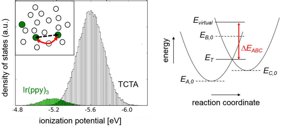
We present a workflow for simulations of multilayer OLED stacks in which microscopic rates of processes involving charges and excitons are computed from first principles. The multiscale approach covers the generation of atomistic morphologies of disordered organic materials, determination of their electronic properties, and finally simulation of charge transport and excitonic processes using kinetic Monte Carlo (kMC). Applying the workflow to undoped layers made up of various organic compounds as well as prototypical OLED emission layers consisting of TCTA doped with Ir(ppy)3, we find remarkable agreement with experimental field-dependent mobility measurements as well as triplet-triplet annihilation (TTA) and triplet-polaron quenching (TPQ) rates extracted from photoluminescence quenching experiments. To demonstrate how this workflow may help understand and optimize microscopic processes underlying OLED performance, we show that, for a simplified lattice system, TPQ becomes the efficiency bottleneck at high current densities and can be significantly reduced by increasing the host material’s electron affinity.
Toward Design of Novel Materials for Organic Electronics
Materials for organic electronics are presently used in prominent applications, such as displays in mobile devices, while being intensely researched for other purposes, such as organic photovoltaics, large-area devices, and thin-film transistors. Many of the challenges to improve and optimize these applications are material related and there is a nearly infinite chemical space that needs to be explored to identify the most suitable material candidates. Established experimental approaches struggle with the size and complexity of this chemical space. Herein, the development of simulation methods is addressed, with a particular emphasis on predictive multiscale protocols, to complement experimental research in the identification of novel materials and illustrate the potential of these methods with a few prominent recent applications. The potential of machine learning and methods based on artificial intelligence is discussed to further accelerate the search for new materials.
Charge Transport by Superexchange in Molecular Host-Guest Systems
Charge transport in disordered organic semiconductors is generally described as a result of incoherent hopping between localized states. In this work, we focus on multicomponent emissive host-guest layers as used in organic light-emitting diodes (OLEDs), and show using multiscale ab initio based modeling that charge transport can be significantly enhanced by the coherent process of molecular superexchange. Superexchange increases the rate of emitter-to-emitter hopping, in particular if the emitter molecules act as relatively deep trap states, and allows for percolation path formation in charge transport at low guest concentrations.
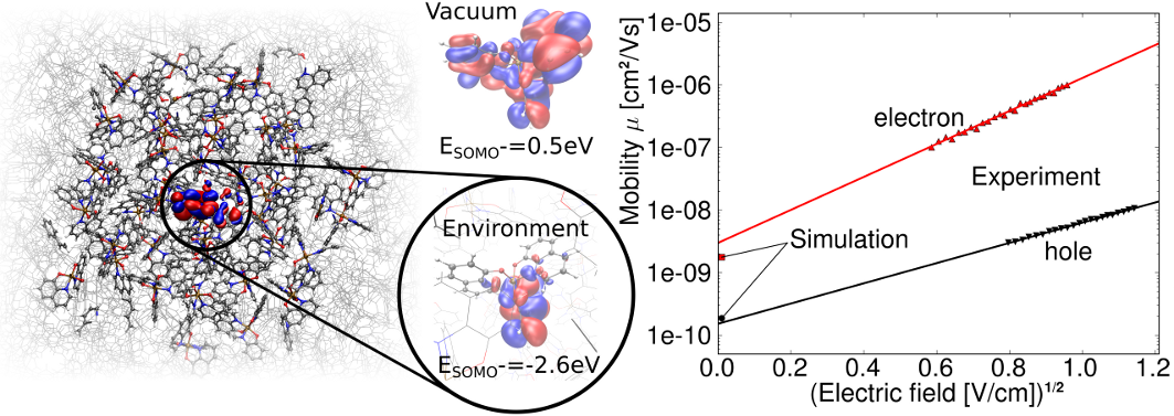
Molecular origin of the charge carrier mobility in small molecule organic semiconductors
A first principles based multiscale model is presented, which accurately predicts charge carrier mobility of different materials varying over ten orders of magnitude. The model allows for the decomposition of the carrier mobility into molecule-specific quantities. The availability of fast and parameter-free screening tools to compute macroscopic materials properties may enable in-silico screening of the chemical compound space for the development of highly efficient opto-electronic devices.
Influence of meso and nanoscale structure on the properties of highly efficient small molecule solar cells
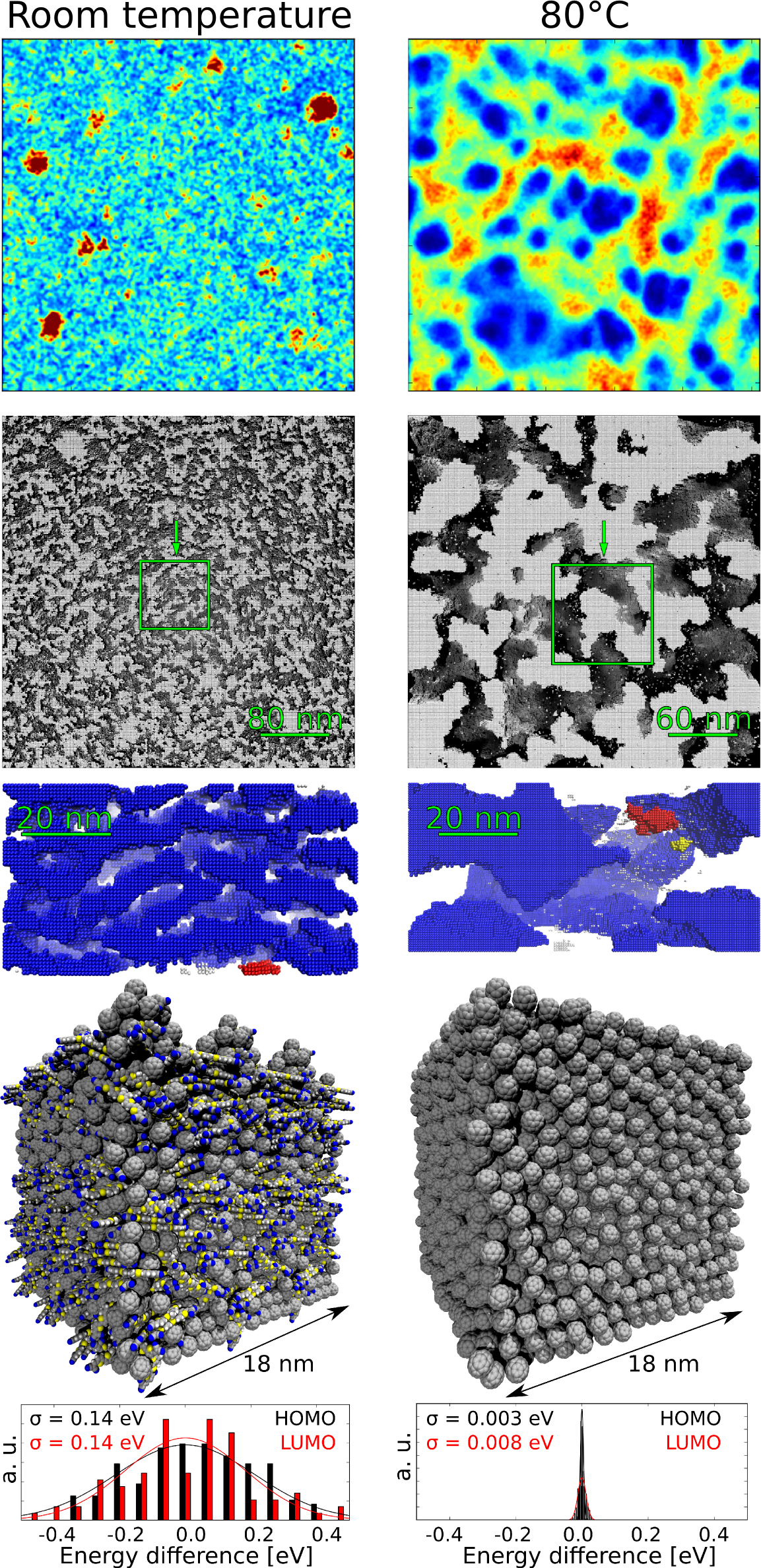
The nanoscale morphology of the bulk heterojunction absorber layer in an organic solar cell (OSC) is of key importance for its efficiency. The morphology of high performance vacuum-processed, small molecule OSCs based on oligothiophene derivatives (DCV5T-Me) blended with C60 on various length scales is studied. The analytical electron microscopic techniques such as scanning transmission electron microscopy, energy dispersive X-ray spectroscopy, highly sensitive external quantum efficiency measurements, and meso and nanoscale simulations are employed. Unique insights into the relation between processing, morphology, and efficiency of the final devices are obtained. It is shown that the connectivity of the oligothiophene-C60 network is independent of the material domain size. The decisive quantity controlling the internal quantum efficiency is the energetic disorder induced by material mixing, strongly limiting charge and exciton transport in the OSCs.
Ab Initio Treatment of Disorder Effects in Amorphous Organic Materials: Toward Parameter Free Materials Simulation
 Disordered organic materials have a wide range of interesting applications, such as organic light emitting diodes, organic photovoltaics, and thin film electronics. To model electronic transport through such materials it is essential to describe the energy distribution of the available electronic states of the carriers in the material. Here, we present a self-consistent, linear-scaling first-principles approach to model environmental effects on the electronic properties of disordered molecular systems. We apply our parameter free approach to calculate the energy disorder distribution of localized charge states in a full polaron model for two widely used benchmark-systems (tris(8-hydroxyquinolinato)aluminum (Alq3) and N,N′-bis(1-naphthyl)-N,N′-diphenyl-1,1′-biphenyl-4,4′-diamine (α-NPD)) and accurately reproduce the experimental charge carrier mobility over a range of 4 orders of magnitude. The method can be generalized to determine electronic and optical properties of more complex systems, e.g. guest-host morphologies, organic–organic interfaces, and thus offers the potential to significantly contribute to de novo materials design.