
Liquid Metal Printing with Scanning Probe Lithography for Printed Electronics
-
Author:
Navid Hussain
-
Source:
Dissertation, Karlsruher Institut für Technologie (KIT) (2022)
- Date: 2022
-
In recent years, with the emergence of Industry 4.0, the Internet of Things (IoT), also referred to as the Internet of Everything, is bringing a stream of innovative and intelligent next-generation sensors-based electronics into everyday life. This also demands the fabrication of a massive number of electronic parts, including sensors, actuators, and other components. The available conventional electronics (also referred to as CE) manufacturing has become a highly complicated process requiring intensive investments. As the number of electronics and the demand for new, more advanced electronics increases, there is a greater need to find more efficient ways to produce these electronics. The printed electronics industry is a growing market that could meet this demand, reshaping the future of electronic device fabrication. It allows easy and cost-effective production and enables devices to be fabricated on paper or plastic substrates. On the fabrication side, there are a lot of methods available, and scanning probe lithography-based techniques have always been part of printed electronics and have led to innovations in the field. Although the technology is still young, and the current state of printed electronics at an industrial scale, such as complete integrated circuit fabrication, is limited, the potential applications are still vast.
A key component of the development of printed electronic circuits is the printing of conductive parts and functional materials. Most of the currently available works for conductors have focused on the use of nanoparticle-based inks. The fabrication steps based on these inks are complicated processes as they include annealing and other post-processing steps to make the printed patterns conductive. The use of gallium based at/near room-temperature liquid metals and their direct writing for fully printed electronics is still uncommon, as the combination of the presence of an oxide layer, high surface tensions, and viscosity makes these materials difficult to handle.
To this end, this thesis aims to develop methods for printing materials, including liquid metals that are very hard to be printed with available printing methods, and use those methods to fabricate fully printed electronic devices. It also investigates solutions for the challenges during the printing process, such as the adhesion of ink to the substrate and other deposition-related issues. It also address scientific questions regarding the device stabilities of liquid metal-based printed electronic devices.
Within the presented thesis, a glass capillary-based direct-write method for printing the liquid metal Galinstan was developed. The method was implemented in two ways, first, a high-performance version based on a customized nanolithography setup, but also a high-accessibility micromanipulator-based version allowing "on-the-fly" capillary printing on a wide range of geometries, as exemplified by the example of vertical, recessed surfaces as well as stacked 3D scaffolds as hard-to-access surfaces. The thesis explores the potential use of these methods for the fabrication of fully printed liquid metal-enabled devices, including resistors, microheaters, p–n diodes, and field effect transistors. All of these electronic devices are extensively characterized. The fabricated microheater structures are utilized for a heat-triggered microvalve to control the liquid flow in a microchannel. This demonstration and the ease of fabrication show that the concept can also be extended to other applications, e.g., on-demand microheater fabrication for in-situ scanning electron microscopy experiments.
Additionally, this work shows how PMMA encapsulation can act as an effective barrier against oxygen and moisture and is feasible mechanical protection of these liquid metal-based printed electronic devices. Overall, the single integrated fabrication flow and device functionality demonstrate that the potential of liquid metal printing in printed electronics is much greater than just the use as a connector between conventional electronic devices.
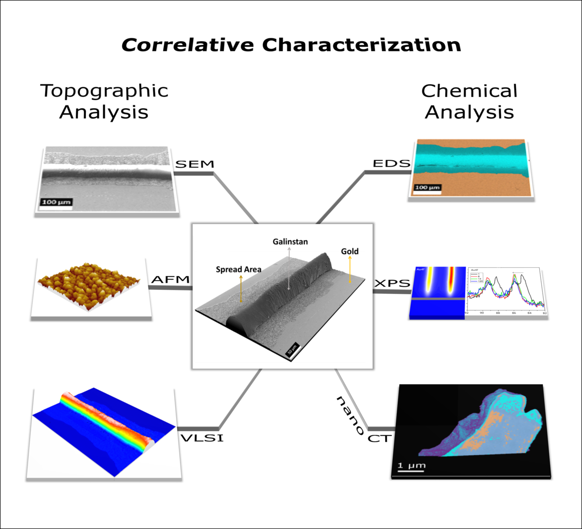
Aside from the development of printing methods and fabrication of electronic devices, the thesis also discusses corrosion and additional alloying of conventional metal electrodes in contact with liquid metal that could compromise device stability. For this, a correlated material interaction study of printed Galinstan and gold electrodes was implemented. In-depth characterization of the spreading process of liquid metal lines on gold films has been achieved through the combined application of optical microscopy, vertical scanning interferometry, scanning electron microscopy, x-ray photon spectroscopy, and atomic force microscopy. This study reveals a differential spread of the different components of the liquid metal and the formation of intermetallic nanostructures on the surrounding gold film surface. Based on the obtained time-dependent correlated characterization results, a model for the spread process based on liquid metal penetration is proposed. In addition, to provide a complementary perspective on the internal nanostructure, X-ray nanotomography is employed to examine the distribution of gold, Galinstan, and intermetallic phases in a gold wire dipped into the liquid metal. Finally, measurements of resistance on liquid metal lines connecting gold electrodes over time are conducted, which help assess the impact of material interactions on electronic applications.