
SPL for Printed Electronics
Scanning Probe Lithography (SPL) methods offer unique opportunities for printed electronic applications in regard to achievable resolution and material integration. Together with the groups of Dr. Ben Breitung, Prof. Horst Hahn and Prof. Jasmin Aghassi-Hagmann, we explore the potential of SPL for printed electronics by miniaturization of devices, workflows for materials and inks that are not processable in standard lithography approaches and minimizing processing steps by reducing the number of involved lithography technologies.
Selected Publications
Printing Technologies for Integration of Electronic Devices and Sensors
T. T. Baby, G. C. Marques, F. Neuper, S. A. Singaraju, S. Garlapati, F. von Seggern, R. Kruk, S. Dasgupta, B. Sykora, B. Breitung, P. A. Sukkurji, U. Bog, R. Kumar, H. Fuchs, T. Reinheimer, M. Mikolajek, J. R. Binder, M. Hirtz, M. Ungerer, L. Koker, U. Gengenbach, N. Mishra, Patric G., M. Tahoori, J. Aghassi Hagmann, H. von Seggern, H. Hahn
Functional Nanostructures and Sensors for CBRN Defence and Environmental Safety and Security. NATO Science for Peace and Security Series C: Environmental Security. A. Sidorenko, H. Hahn (eds.) Springer Nature B.V. (2020) 1-34, DOI:10.1007/978-94-024-1909-2_1
Functionalization of Photonic Structures
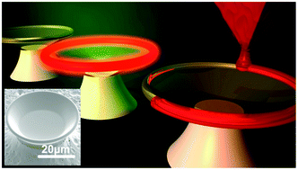
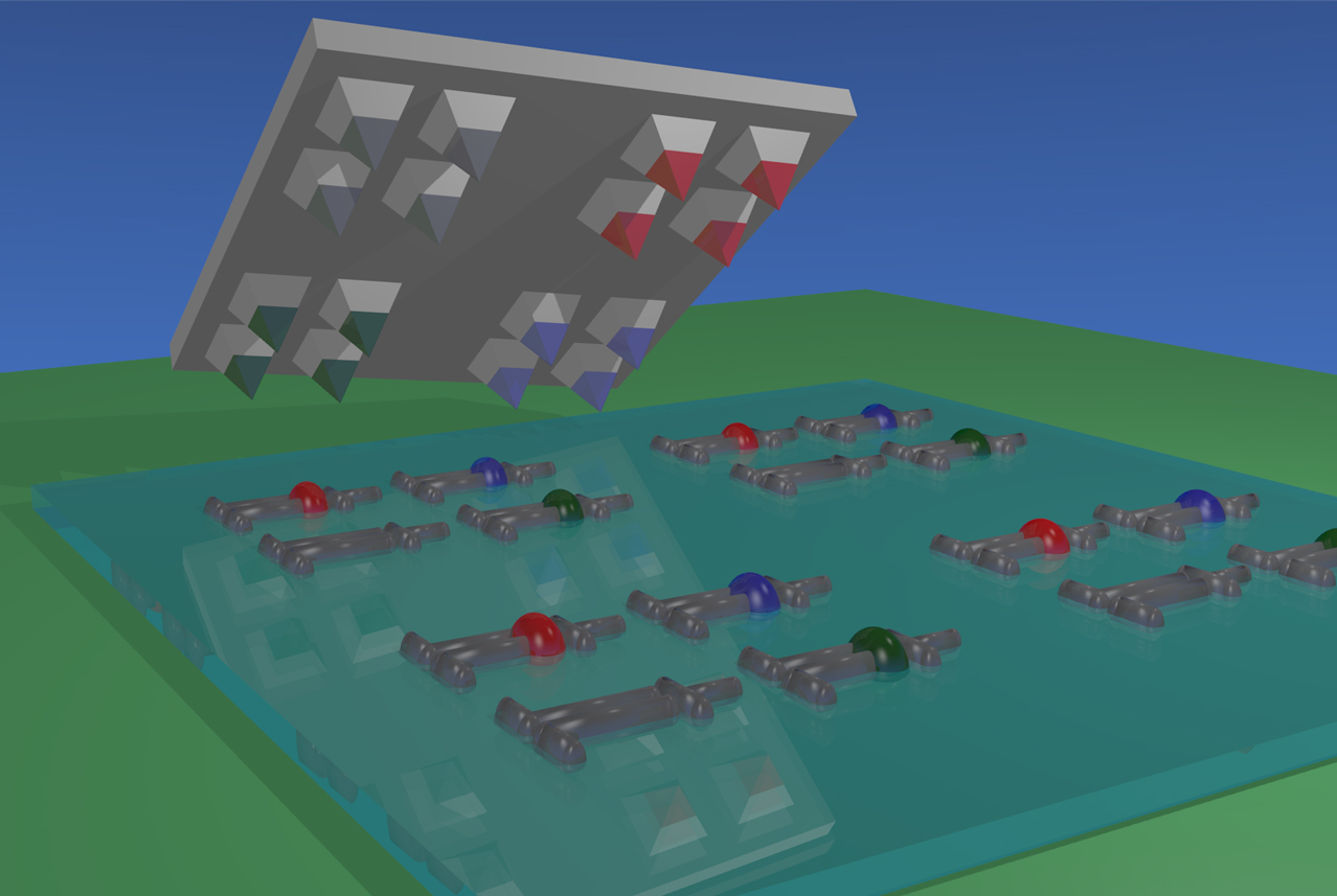
DPN can be employed for the direct generation of photonic structures as well as for the post functionalization of sensor devices fabricated by other methods. The high-precision positioning and the ability to write on three dimensional pre-strcutured surfaces opens up additional possibilities to functionalize devices fabricated by standard semiconductor industry processes. By combining the well established methods for device fabrication and the advantages of DPN on regard to materials and parallel writing of different inks, sensors with functionalization not achievable by standard lithography methods can be generated. One example ist the decoration of optical resonator structures with lipids by DPN.
The lipid mixture added to the rims of the goblet structure serves as optical active material as well as specific binding site for target proteins. The so-functionalized goblet structures can then serve as sensors based on the shift in optical properties during protein binding. To enhance throughput and ease alignment procedures, it is also possible to use aligned stamping to apply lipid functionalization.
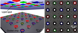
Here, a stamp pad is first generated by multi-color polymer pen lithography (PPL) and subsequently stamped onto a goblet array. A combined fluorescence / bright field image of a functionalized array is shown on the right.
Selected Publications
Large-Scale Parallel Surface Functionalization of Goblet-type Whispering Gallery Mode Microcavity Arrays for Biosensing Applications
U. Bog, F. Brinkmann, H. Kalt, C. Koos, T. Mappes, M. Hirtz, H. Fuchs, S. Köber
Small 10 (2014) 3863-3868, DOI:10.1002/smll.201400813
On-chip microlasers for biomolecular detection via highly localized deposition of a multifunctional phospholipid ink
U. Bog, T. Laue, T. Grossmann, T. Beck, T. Wienhold, B. Richter, M. Hirtz, H. Fuchs, H. Kalt, T. Mappes
Lab Chip 13 (2013) 2701-2707, DOI:10.1039/C3LC50149C
Functionalization of Graphene
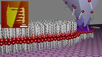
Graphene (and other 2D materials) are of interest for device and research applications as for their unique electronic properties. Often, specific functionalization of the material to tune and taylor these properties is desired, e.g. in sensing, but also for adjusting the interface in regard to adhesion or wetting properties. This can enhance performance in regard to unspecific adhesion ("anti-fouling") and thus enhance sensing capability.
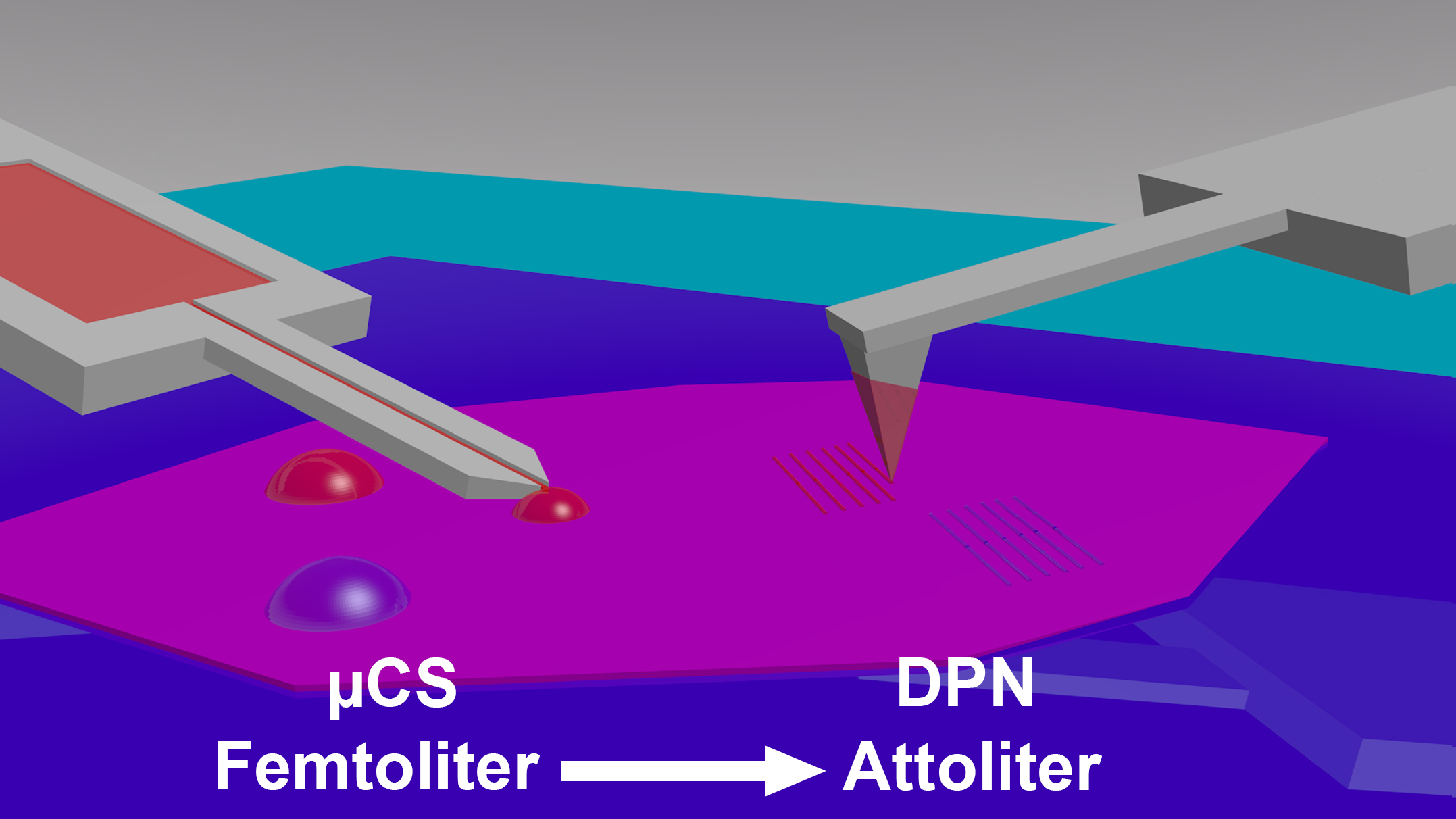
The SPL methods allow to do these functionalizations highly site-specific and in high resolution. By utilizing different methods, femto- to attoliter sized volumes of reactive solutions can be deposited on the 2D material in order to allow chemical reactions taking place. Also non-covalent modifications with small molecules or phospholipid membranes are feasible with the SPL approach.
Selected Publications
Multiplexed biomimetic lipid membranes on graphene by dip-pen nanolithography
M. Hirtz, A. Oikonomou, T. Georgiou, H. Fuchs, A. Vijayaraghavan
Nat. Commun. 4 (2013) 2591, DOI:10.1038/ncomms3591
Attoliter Chemistry for Nanoscale Functionalization of Graphene
M. Hirtz, S. Varey, H. Fuchs, A. Vijayaraghavan
ACS Appl. Mater. Interfaces 8 (2016) 33371-33376, DOI:10.1021/acsami.6b06065
Self-limiting multiplexed assembly of lipid membranes on large-area graphene sensor arrays
M. Hirtz, A. Oikonomou, N. Clark, Y. Kim, H. Fuchs, A. Vijayaraghavan
Nanoscale 8 (2016) 33371-33376, DOI:10.1039/C6NR04615K
Biomimetic Phospholipid Membrane Organization on Graphene and Graphene Oxide Surfaces: a Molecular Dynamics Simulation Study
N. Willems, A. Urtizberea, A. F. Verre, M. Iliut, M. Lelimousin, M. Hirtz, A. Vijayaraghavan, M. S. P. Sansom
ACS Nano 11 (2017) 1613-1625, DOI:10.1021/acsnano.6b07352