
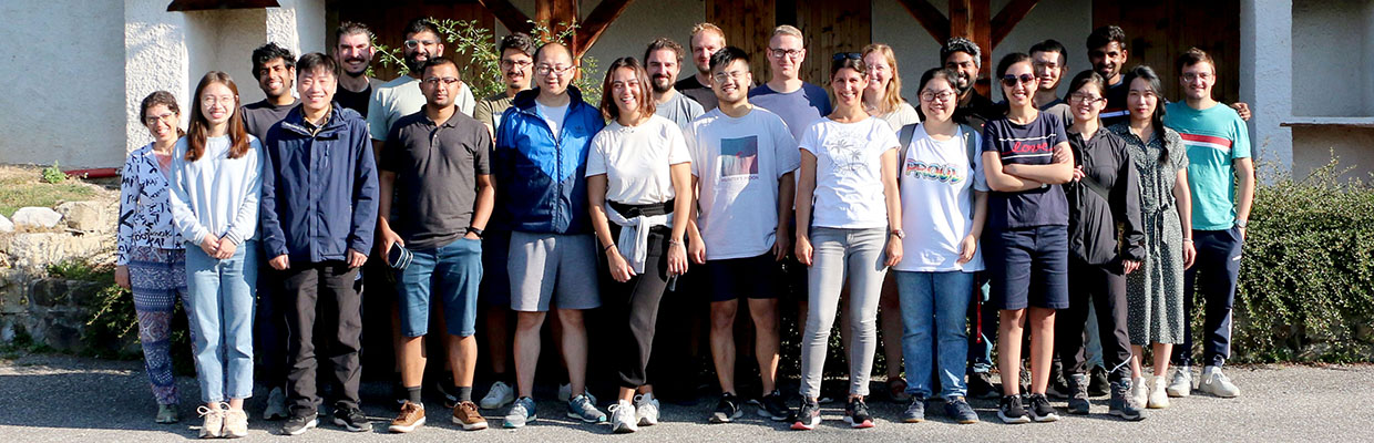
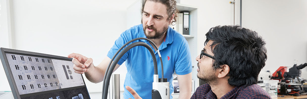
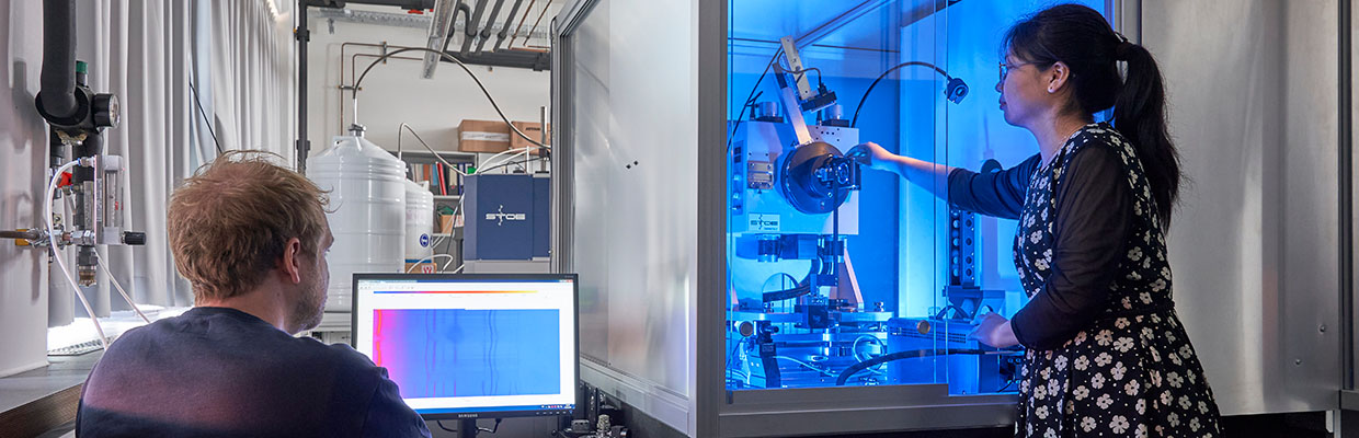
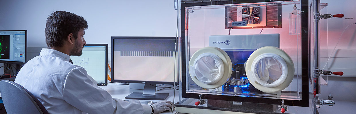
Welcome to the research unit of Prof. Aghassi-Hagmann in which we explore electronic devices and systems in future technologies with a special focus on printed electronics. We are an interdisciplanary group of electrical engineers, physicists, material scientists and computer scientists located at KIT campus north working on printed materials, novel nanomaterials, micro/nano-structured devices, additive manufacturing techniques and systems in the field of future electronic technologies. We strive for gaining understanding from materials to device level and to develop solutions for electronic, bioelectronic and energy applications.
If you are interested in our research or seek job oppertunities do not hesitate to contact us.
NeuroConnect 2026 | Organoid Neurophysiology  Workshop
26.03.2026 | Karlsruhe
Prof. Dr. Jasmin Aghassi-Hagmann is co-organizing the upcoming Workshop NeuroConnect 2026:
To find better treatments for brain disorders, we aim to develop enhanced in vitro models of the human brain and mature them through electrical stimulation. A 1-day workshop with international experts and the local scientific community in the Rhine valley in Freiburg and Karlsruhe on 26 March 2026 will kickstart this research direction.
More information and registration
KIT and Intel Develop Microchip for Research-oriented Teaching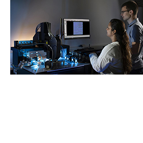
KIT is the first German university to develop a test chip together with the semiconductor manufacturer Intel.
Students and researchers at the Karlsruhe Institute of Technology (KIT), together with the US chip manufacturer Intel, have developed a microchip designed for research and teaching - starting from the design process to tape-out and eventually raw die characterization. The chip is called KIT “Callisto” with a total area of four square millimeters and exploits Intel 16 which is Intel’s CMOS Finfet-16nm transistor technology.
Read Article
3D Matter Made to Order special issue: Advanced  Functional Materials 2024)
The Cluster of Excellence 3D Matter Made to Order (3DMM2O) establishes scalable digital 3D additive manufacturing with feature sizes on the molecular or nanometer scale all the way up to object sizes on the micro- or macroscale, and applies cutting-edge versions of this technology to answer previously inaccessible scientific questions in the technical and the life sciences.
Read more
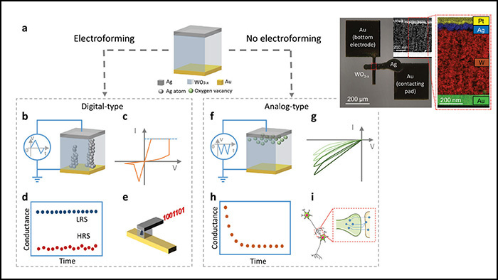
An inkjet-printed tungsten oxide memristor is developed, which exhibits either digital-type switching for data storage or analog-type memristor behavior for neuromorphic computing.
Advanced Functional Materials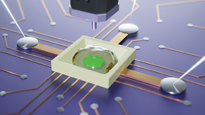
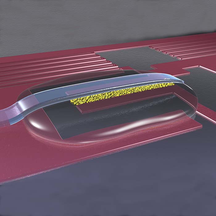
Depiction of a printed biolelectronic device in which a cell and electronics form a hybrid structure.
Advanced Functional Materials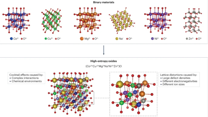
The transformation of binary materials (simple oxides) into a high-entropy material.
Nature Reviews Materials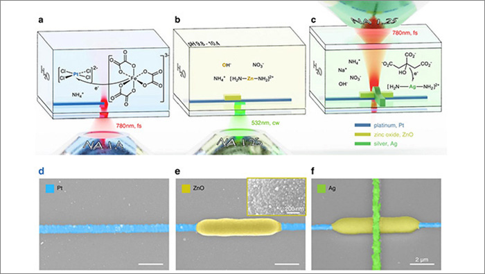
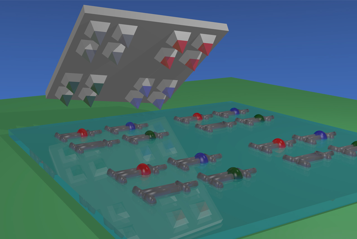
Laser printing with three different inks, for the semiconductor ZnO and the metals Pt and Ag, as a facile process for fabricating printed functional electronic devices with minimum feature sizes below 1 µm.
Nature Communications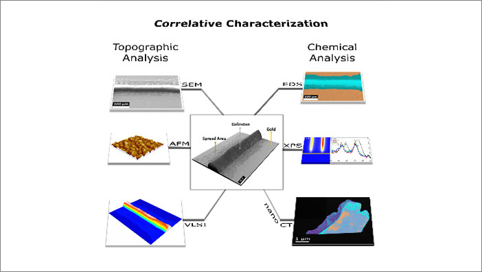
A comprehensive, correlated study of the interaction of liquid metals with gold as conventional electrode material, yielding crucial information on the interaction processes.
Small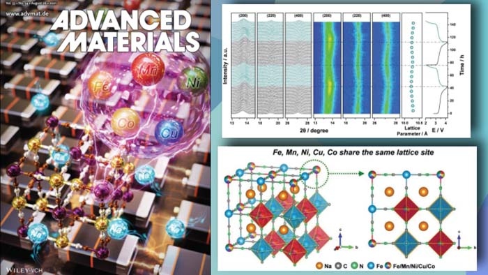
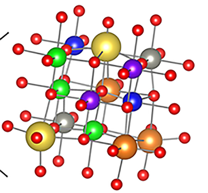
A new approach is presented to substantially improve the electrochemical properties of PBAs by introducing high entropy into the crystal structure.
Advanced Materials