
Graphitic Materials
In collaboration with INT internal and a number of external groups, we are characterizing structure and defects of carbon nanotubes (CNTs) and graphene operating the Titan at low acceleration voltage to minimize damage to the graphitic materials.
1. In situ observation of structural changes during graphitization
Graphitization of polymers is an effective way to synthesize nanocrystalline graphene on different substrates with tunable shape, thickness and properties. The catalyst free synthesis results in crystallite sizes on the order of a few nanometers, significantly smaller than commonly prepared polycrystalline graphene. Even though this method provides the flexibility of graphitizing polymer films on different substrates, substrate free graphitization of freestanding polymer layers has not been studied yet. In collaboration with Prof. Ralph Krupke group, we are studying the thermally induced graphitization and domain growth of free-standing nanocrystalline graphene thin films using in situ TEM techniques. High resolution transmission electron microscopy (HRTEM), selected area electron diffraction (SAED) and electron energy loss spectroscopy (EELS) techniques are used to analyze the graphitization and the evolution of nanocrystalline domains at different temperatures by characterizing the crystallinity and domain. In situ graphitization provided high quality large area thin free standing films, eliminating possible artefacts associated with the transfer process. In situ graphitization of these thin films helped us to understand the process of graphitization in detail. In situ studies showed that the graphitization process is highly dynamic with number of intermediate reactions leading to the formation of different carbon nanostructures. A two stage growth mechanism was identified where at an intermediate temperature (600-1000 ºC) crystallite growth is by consumption of amorphous carbon around the crystallites and at high temperatures (1000- 1200 ºC) growth proceeds by merging of crystallites (figure.1). This occurs either by attachment of small domains to active edges of other domains and by a catalyst free transformation on the top of another graphitic layer. This catalyst free transformation forms new small graphitic structures with different size shape and mobility (figure 2). Some of these carbon nano structures are highly mobile on the top of already graphitized layers which enable us to study the interaction of these structures with the graphitic substrate.
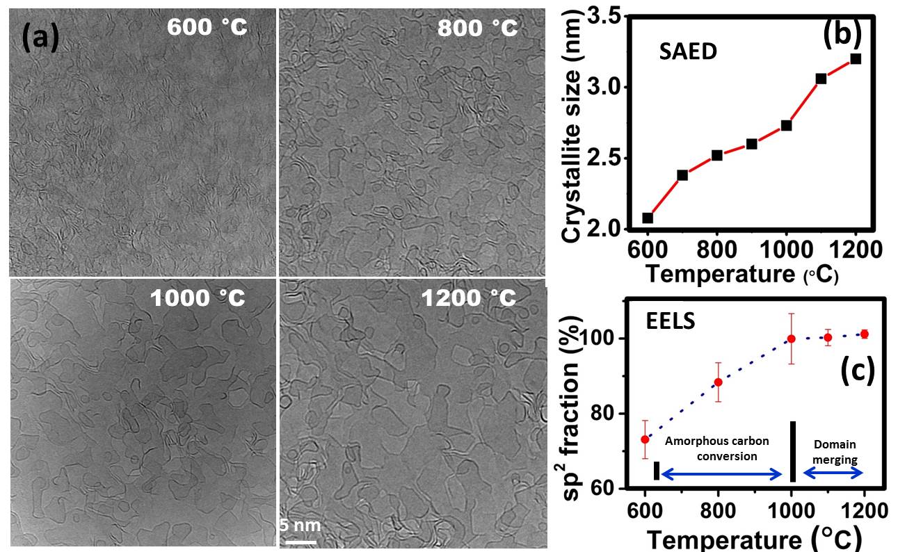
Figure 1.1: (a) the evolution of domains, (b) crystallite size evolution during hating and (c) the sp2 content at different temperatures. The sp2 content increases from 600 ºC to 1000 ºC and saturates indicating that the amorphous carbon is completely consumed at 1000 ºC and further domain growth is facilitated by merging of domains
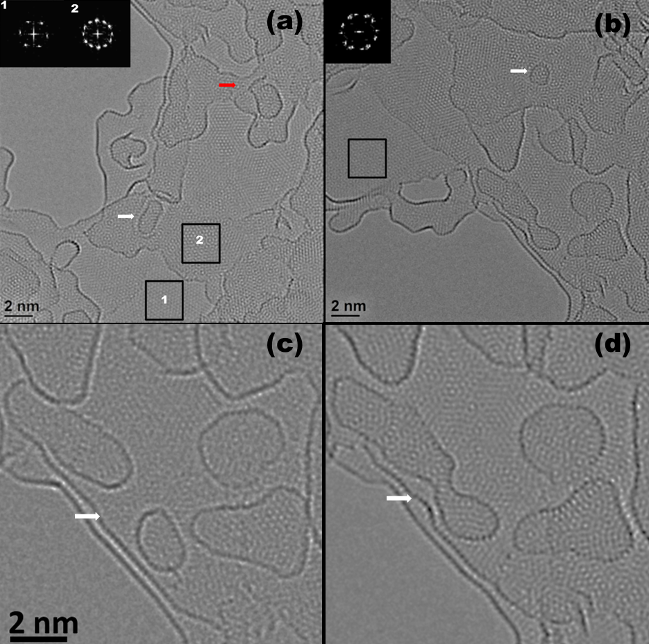
Figure 2.1: In situ TEM observation of structural changes during thermal annealing of few layer graphene at 1200C.
Video 1.1: Shape changes and motion of a small graphene flake at 1200 ºC.
HRTEM investigations revealed the formation of different carbon nanostructures during the graphitization and the dynamics and interaction of these structures with graphitic substrate differ a lot. At high temperatures, these nanostructures are mobile and highly reactive leading to different atomic level interactions and dynamics (video 1. or figure 1.3). A detailed in situ study is being carried out to understand the process of formation of different carbon nanostructures, temperature dependence of the formation mechanisms, stability of the nanostructures at higher temperatures and the interactions with the graphitic substrate at different temperatures.
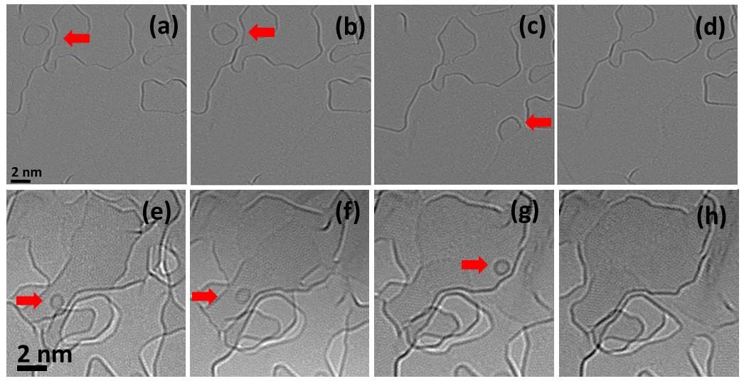
Figure 3: (a-d) migration and merging of a graphitic flake at 1200 ºC.
Details have been published at:
- Understanding the graphitization and growth of free-standing nanocrystalline graphene using in situ transmission electron microscopy
C.N. Shyam Kumar, Venkata Sai Kiran Chakravadhanula, Adnan Riaz, Simone Dehm, Di Wang, Xiaoke Mu, Benjamin Flavel, Ralph Krupke and Christian Kübel
Nanoscale 2017, 9, 12835-12842, DOI:10.1039/c7nr03276e.

This project is partially third-party funded by the DAAD PhD scholarship of Shyam Kumar Neelakandhan.
2. Vertically aligned MWCNTs grown by plasma enhanced chemical vapor deposition (PECVD)
The interplay between substrate, catalyst and temperature on the growth and structure of MWCNTs has been studied in collaboration with Dr. Mireille Gaillard at the University of Orleans as part of an EUMIAfab project funded in the 7th Framework by the EU.
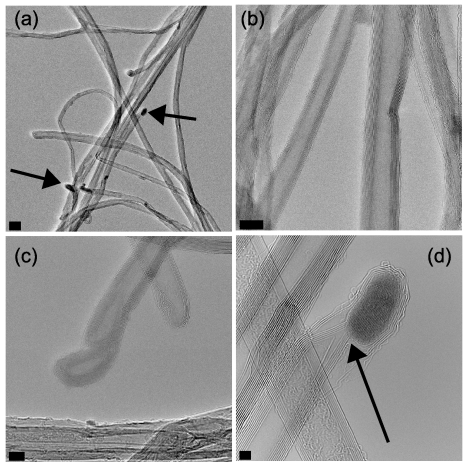
Among the different techniques available to obtain thin films of densely packed vertically aligned carbon nanotubes (CNTs), plasma-enhanced chemical vapor deposition (PECVD) is especially useful because of its ability to significantly reduce the growth temperature. This is particularly important for the integration of CNTs in microelectronics, optoelectronic components, and micromechanical structures. However, PECVD requires the deposition of a catalyst to trigger the growth mechanisms, which increases the process complexity. Numerous studies have been dedicated to the growth mechanisms present during the PECVD process and to understanding the influence of different experimental parameters on the resulting CNTs. It is well-known that the supported catalyst has a much more active CNT growth when it has a nanoparticle (NP) shape. The growth results are influenced e.g. by the catalyst type and composition, as well as by the NP size, pattern geometry, density, and crystallographic orientation. The experimental conditions under which the NP catalysts are produced also influence the CNT structure and growth. We studied vertically aligned CNTs by HRTEM where we focused on the catalyst nanoparticle shape and localization within the CNTs with respect to the support layer and growth temperature to better understand the influence of the catalyst on the CNT growth.
|
Figure 2.1 shows typical TEM images of MWCNTs grown from an Fe/Si3N4 system with a well-defined wall structure typically consisting of 3-10 graphene layers (scale bars 20 nm (a), 10 nm (b), 5 nm (c), and 2 nm (d)). Both, CNTs where the top end is filled with catalyst nanoparticles (arrows in a) as well as CNTs where the top end is empty (c) are observed experimentally indicating that both tip and base growth modes are possible simultaneously. Figure 1d shows a HRTEM image revealing details of the graphene layers growing perpendicular to the inner surface of the catalyst nanoparticle. |
Figure 2.2 shows a BF-TEM image and the corresponding EFTEM maps of catalyst nanoparticles inside a MWCNT representative of the typical alloyed nanoparticles observed when grown with a mixture of Ni and Fe as catalyst.
|
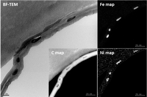
Under the conditions used in this study CNT growth was only observed for the Fe/Si3N4 system and the Ni/TiN system, whereas very limited growth was achieved for the Ni/Si3N4 and the Fe/TiN system. However, when using a bimetallic catalyst Fe:Ni with a nominal atomic ratio of 2:1, CNT growth was observed on both substrates. EFTEM studies (Figure 2) of the particles present inside and at the CNT tip always shows bimetallic particles present, although the atomic ratio is varying between particles.
Details of this study have been published and are available at
- Gaillard et al.: High-resolution TEM observations of multiwalled CNT microstructures, J. Vac. Sci. Technol. B, Vol. 31(3), 2013, 031805, DOI: 10.1116/1.4804543.
3. Impact of sonication pretreatment on carbon nanotubes
In collaboration with Dr. Marta Rossel and Dr. Rolf Erni from the EMPA, we performed a TEM study of the effects of sonication treatment on the structure of CNTs. Sonication treatments are commonly used for debundling and dispersing carbon nanotubes (CNTs) in liquid media prior to chemical functionalization. However, this step may lead to the stripping of the outer graphitic layers and the scission of the CNTs, and can therefore have a deleterious effect on the achievable properties of the functionalized CNTs. Thus, knowledge on the structural integrity of the modified CNTs is required to understand its influence on the device performance of hybrid nanocarbon-based composites. Here we report on the impact of a sonication pretreatment on the structure of multi-walled CNTs, and on the role of the induced modifications on the subsequent attachment of ferromagnetic Fe3O4 nanoparticles. Decoration of the CNTs with Fe3O4 nanoparticles is achieved by a microwave-assisted synthesis route involving the reaction of iron acetylacetonate with 2-pyrrolidinone. Employing a combination of atomic resolution transmission electron microscopy at our facility and EELS/EFTEM analysis at EMPA, we provide evidence that significant degradation of the CNT structure takes place during the dispersion process. Moreover we find that the sp2 system is more heavily disrupted at the interface between the CNTs and the surface-deposited nanoparticles suggesting that nucleation of Fe3O4 preferentially occurs at the nanotube defect sites.
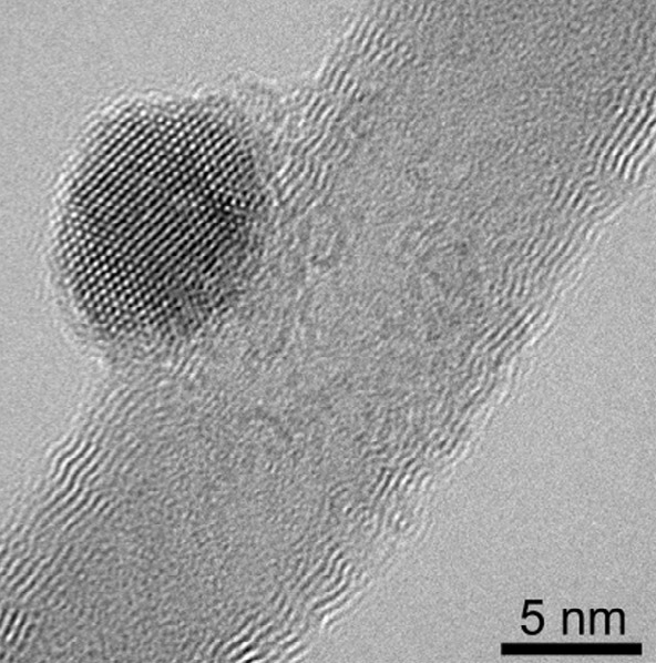
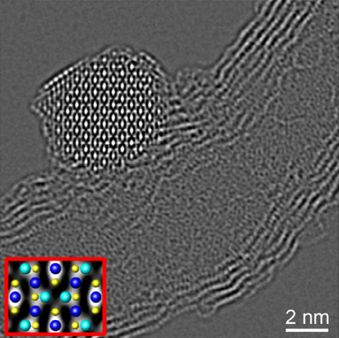
Fig 3.1: HRTEM image and focal series reconstruction of the MWCNTs with Fe3O4 nanoparticles attached.
Details of this study have been published and are available at
-
M.D. Rossell, C. Kübel, G. Ilari, F. Rechberger, D. Koziej, M. Niederberger, R. Erni "Impact of sonication pretreatment on carbon nanotubes: a transmission electron microscopy study", Carbon, 2013, 61, 404-411; DOI: 10.1016/j.carbon.2013.05.024.
4. Macroscopic 3D Nanographene
Surface-dominated bulk materials provide the unique opportunity to dynamically control their physical bulk properties by modification of their surfaces through interfacial phenomena. Generating a sizable effect, however, requires that surface atoms constitute a large fraction of the total number of atoms. Jürgen Biener and coworkers at the Lawrence Livermore National Laboratory developed a “top down” strategy to fabricate graphene-based bulk materials from low-cost polymer-derived carbon foams through the controlled removal of carbon atoms to form a network composed of both amorphous carbon and graphite nanoplatelets. The application of the bulk 3D nanographenes, e.g., as actuators have been explored by the groups of Prof. Horst Hahn at KIT and Prof. Jörg Weißmüller at TU Hamburg-Harburg. The structure of this new type of material has been characterized using a combination of HRTEM and EELS spectroscopy, revealing a graphitic electronic structure with on average 2-3 stacked graphene layers despite the strongly bend structure observed in HRTEM.
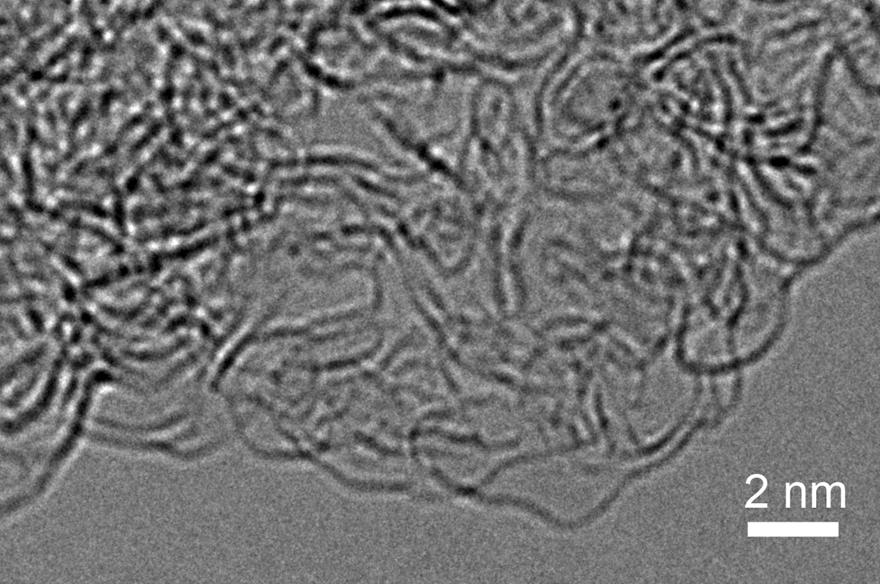
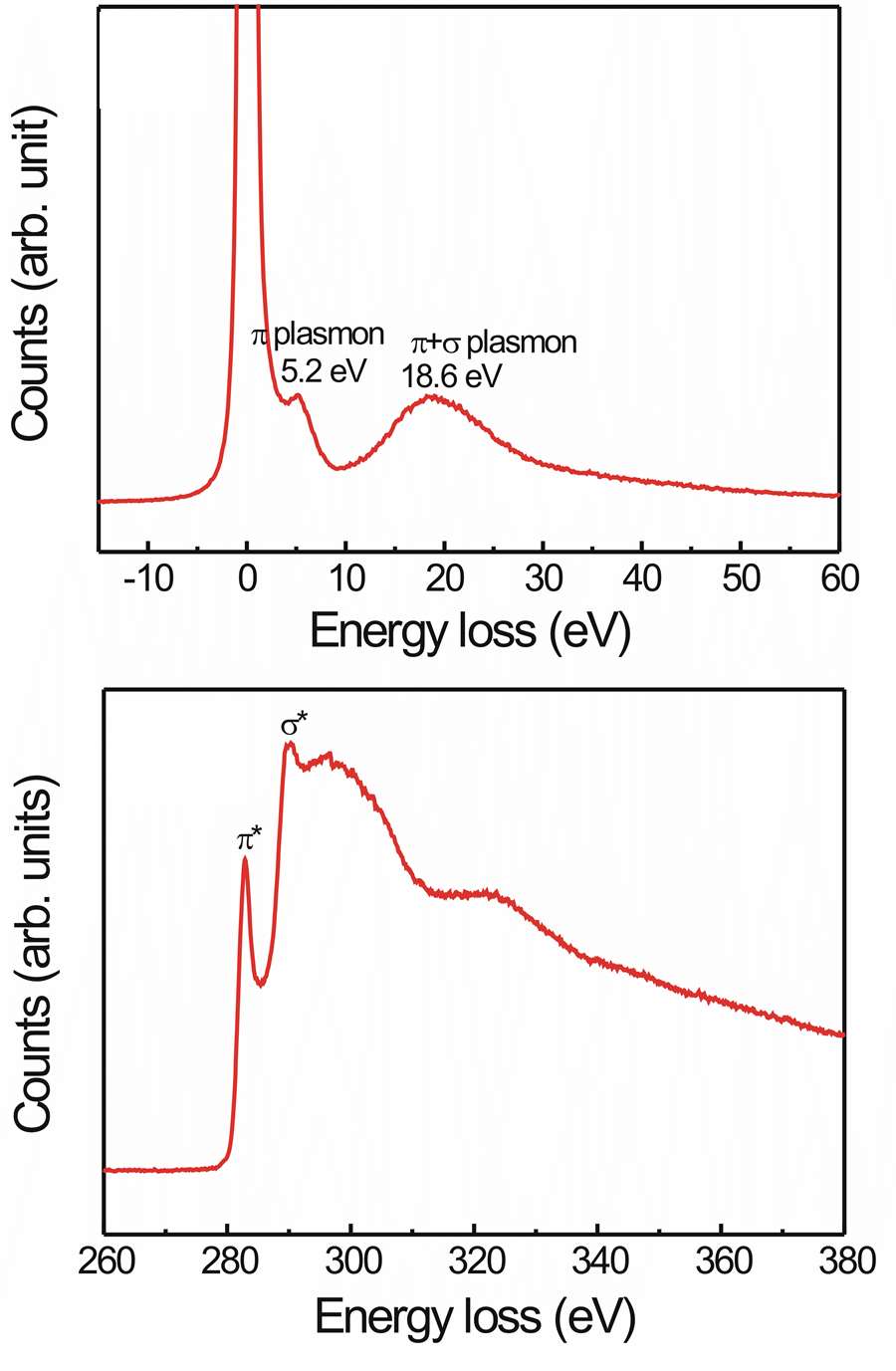
Fig. 4.1: HRTEM imaging and EELS analysis of 3D nanographene.
Details of this study have been published and are available at
-
J. Biener, S. Dasgupta, L Shao, D. Wang, M. Worsley, A. Wittstock, J.R. Lee, M. Biener, C. Orme, S.O. Kucheyev, B.C. Wood, T.M. Willey, A.V. Hamza, J. Weissmüller, H. Hahn, T. Baumann, "Macroscopic 3D Nanographene with Dynamically Tunable Bulk Properties", Adv. Mat., 2012, 24, 5083-5087, DOI: 10.1002/adma.201202289.