
ACOM-STEM
The direct structural characterization of randomly oriented bulk nanocrystalline metals using electron microscopy techniques is very challenging as the contrast in classical BF/DF-TEM images is dominated by a mixture of crystal orientation, bending, defects and strain which is difficult to separate. HRTEM of individual crystals is possible, but time consuming to get the crystallite well-oriented and is limited to just one grain at a time. Therefore, we have been looking into alternative techniques for quantitative characterization of the grain structure in nanocrystalline materials.
NanoMegas has commercialized a solution for Automated Crystal Orientation Mapping (ACOM), where based on a 2D array of diffraction patterns, crystal orientation maps are generated. For this, the electron beam is focused to a small spot of 1-1.5 nm diameter and scanned across the sample with a diffraction pattern recorded for every pixel (Fig. 1a). The diffraction patterns are then cross-correlated with a bank of simulated diffraction patterns representing all possible phases and crystal orientations. The best phase and orientation is determined as the orientation with the highest cross-correlation index and the accuracy/reliability of this identification can be judged based on the cross-correlation index and the ratio of the highest and the second highest cross-correlation index as a measure for the uniqueness of the solution (Fig. 1b).
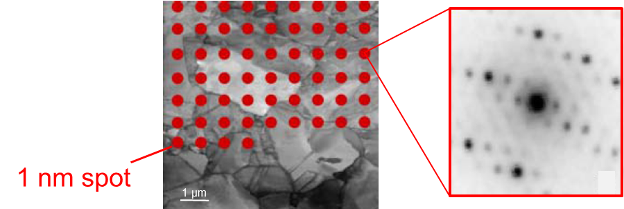
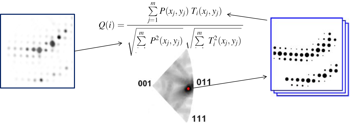
Fig. 1: a) Schematic representation of scanning a sample with a small beam; b) pattern matching of an experimental diffraction pattern with a bank of simulated patterns to determine the local orientation.
We are using the NanoMegas system on our FEI Tecnai F20ST and are operating the microscope in up-STEM mode in order to be able to acquire fast STEM reference images and maintain an almost parallel illumination (semi-convergence angle ~1mrad) for high quality diffraction patterns.
For a quantitative evaluation of the orientation maps, we are performing a brute force optimization of the indexing parameters to obtain the best combination of reliability and correlation index for our crystal orientation maps. Afterwards, the maps are further filtered to reduce noise in the orientation maps using an extension of a median filter modified to deal with higher dimensional data (Euler angles). Finally, grains and crystallites are automatically detect using the freeware Mtex, which has been modified with additional routines for data quantification enabling texture analysis, anisotropic grain size analysis and detection of CSL boundaries.
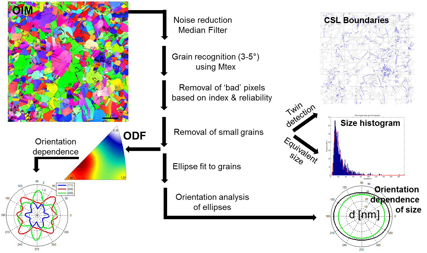
Fig. 2: Schematic representation of the data quantification and analysis process for ACOM-STEM
The crystal orientation maps obtained this way can be fully quantified and the results are in good agreement, e.g. with grain sizes and texture measured using X-ray diffraction techniques (single-line deconvolution) at a synchrotron source. The results below show the grain size and texture evolution of a electrodeposited nanocrystalline nickel film before and after compression by 20%. Both techniques clearly reveal the grain growth perpendicular to the compression direction, whereas the grain size in compression direction stays almost constant. The texture started out with an (fairly) isotropic distribution and after compression the characteristic six-fold symmetry of the 111-peak can be seen ... the symmetry is more pronounced in the X-ray analysis, where millions of crystals are averaged, compared to the quantitative ACOM-STEM analysis where typically 500-1000 grains are analyzed. Nevertheless, the overall trend is very similar.
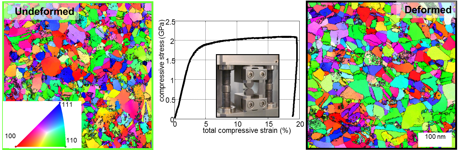
Fig. 3: ACOM orientation maps determined before (left) and after compression (right) of nc Ni.
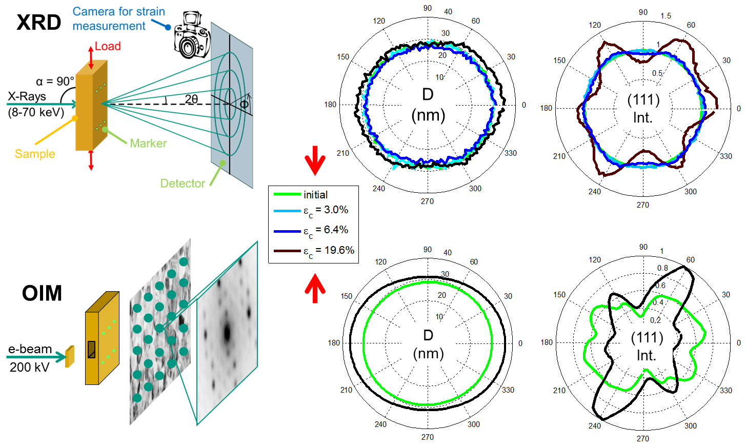
Fig. 4: Comparison of the XRD and ACOM orientation mapping showing good qualitative and quantitative agreement for the grain size and texture evolution during straining.
This work is done in close collaboration with the groups of Patric Gruber, Oliver Kraft and Horst Hahn at KIT and Rainer Birringer at the Universität des Saarlandes. Kerstin Schüler at the Universität des Saarlandes prepared the electrodeposited nickel and Veijo Honkimäki was responsible for the beamline D15 at the ESRF. Furthermore, support for the ACOM analysis by Edgar Rauch and Muriel Veron at the SIMAP Laboratory Grenoble is gratefully acknowledged.
More details on this work have been published at
-
J. Lohmiller, M. Grewer, C. Braun, A. Kobler, C. Kübel, V. Honkimäki, O. Kraft, R. Birringer, P.A. Gruber, "Untangling dislocation and grain boundary mediated plasticity in nanocrystalline Nickel", Acta Mat., 2014, 65, 295-307; DOI: 10.1016/j.actamat.2013.10.071.
-
A. Kobler, A. Kashiwar, H. Hahn, C. Kübel, "Combination of in-situ straining and ACOM TEM: a novel method for analysis of plastic deformation of nanocrystalline metals", Ultramicroscopy, 2013, 128, 68-81; DOI: 10.1016/j.ultramic.2012.12.019.
-
In situ observation of deformation processes in nanocrystalline face-centered cubic metals
A. Kobler, C. Brandel, H. Hahn, C. Kübel, Beilstein Journal of Nanotechnology, 2016, 7, 572–580; DOI: 10.3762/bjnano.7.50. -
Challenges in Quantitative Crystallographic Characterization of 3D thin films by ACOM-TEM, A. Kobler, C. Kübel, Ultramicroscopy, 2017, 173, 84-94; DOI: 10.1016/j.ultramic.2016.07.007.
This project is funded by the DFG as part of the DFG Forschergruppe 718 and the Karlsruhe Nano Micro Facility (KNMF).