
In-situ Electrical TEM
Solid State Batteries
To better understand the processes during cycling of rechargable batteries, we are developing new preparation and analysis approaches to follow the structural changes in micron sized solid state batteries and half cells in situ. The basic idea is to use FIB preparation to cut a thin cross-section from a solid state battery that is then transferred under (close to) inert conditions onto an electro-contacting TEM holder for in situ analysis using low-dose and low voltage TEM and STEM techniques if needed.
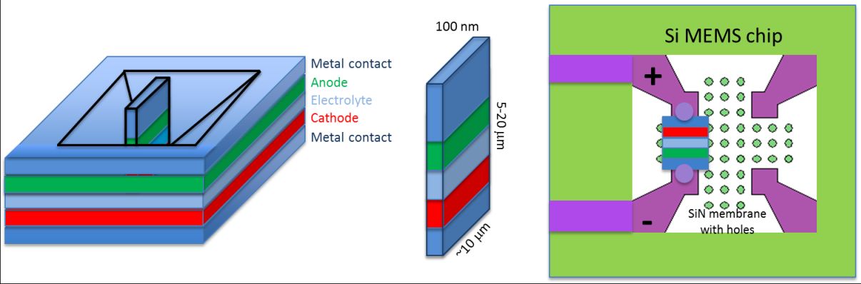
Fig. 1: a) Schematic of a thin film solid state battery with a FIB milling of a thin lamella indicated;
b) schematic and dimensions of a typical TEM lamella based micron sized battery;
c) schematic of the set-up for in-situ analysis of a solid state battery inside the TEM.
The materials that have been recently investigated are solid state fluoride ion batteries in caollaboration with Prof. Max Fichtner's group. For a La0.9Ba0.1F2.9/Bi half-cell and for a MgF2/La0.9Ba0.1F2.9/Cu full cell, we have performed the first successful in situ cycling experiments, where we obtained a reasonable I/V charging/discharging curve and imaged some of the structural and compositional changes during cylcing.
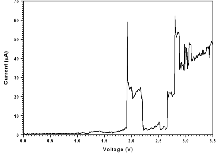
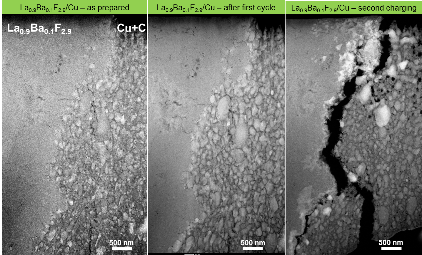
Fig. 2: a) I/V curve obtained during in situ charging of a micron sized La0.9Ba0.1F2.9/Bi half-cell with the main peaks corresponding to Bi oxidation and BiF3 formation; b) morphological changes during cycling of a MgF2/La0.9Ba0.1F2.9/Cu full cell with Cu recrystallization, void formation and finally fracture at the interface between eletrode and electrolyte visible.
Details have been published at
- In situ TEM studies of micron-sized all-solid-state Fluoride Ion Batteries: Preparation, Prospects and Challenges,M. Hammad, V.S.K. Chakravadhanula, M.A. Reddy, C. Rongeat, T. Scherer, H. Hahn, M. Fichtner, C. Kübel, Microscopy Research and Technique, 2016, 79, 615-624; DOI: 10.1002/jemt.22675.
-
First results from in situ transmission electron microscopy studies of all-solid-state fluoride ion batteries
M. Fawey, V.S.K. Chakravadhanula, A.R. Munnangi, C. Ronegeat, H. Hahn, M. Fichtner, C. Kübel
Journal of Power Sources, 2020, 466, 228283; DOI: 10.1016/j.jpowsour.2020.228283.
Radiation Effects on Electrical Properties
Electron beam damage is well known to be critical in in situ battery studies due to the sensitive lithium compounds and the organic electrolytes, even though the detailed effects on the reaction pathways during electrochemical cycling are often not established. In case of metal oxides or semiconductor oxides, electron beam damage is typically only considered to be a significant factor for TEM analysis at very high dose. This is partially because the structural changes due to the electron beam are often difficult to identify clearly, especially in amorphous oxides. However, the electrical response can be drastic, even at very low dose, for both low and high voltage SEM and TEM.
In this work, we attempt to identify the changes in semiconductor and metal oxide systems during electron beam irradiation and correlate them with the electrical changes. We discuss the electron beam induced damage in SiO2, TiO2, and NbxOy as examples to study the damage mechanism, the structural changes induced and, in particular, the effect on the electrical properties.
|
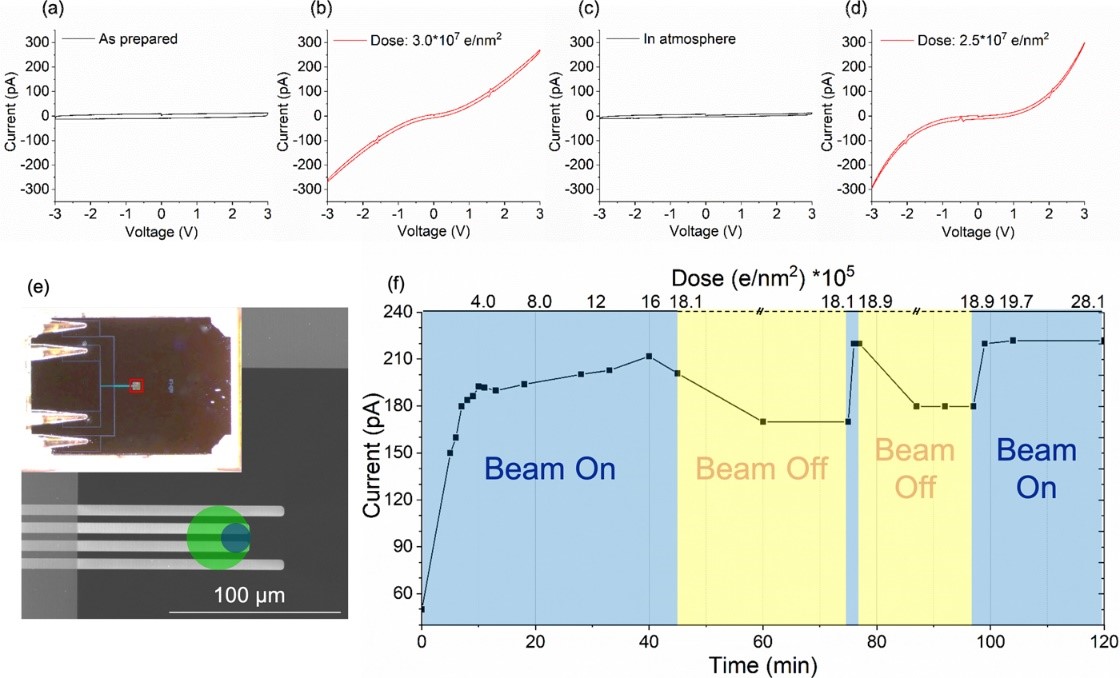
Fig. 3-3. I/V measurement on PECVD deposited SiO2: transformation from insulating (a) to conductive (b) after electron beam exposure (dose ~3 × 10⁷ e/nm2), back to insulator (c) after exposure to atmosphere and finally back to conductive (d) after further electron beam exposure (dose 2.5 × 10⁷ e/nm2). Dose rate: ~670 e/nm2 s. e: Schematic of the electrical chip. The green circle shows the area (D = 36 µm) exposed by the electron beam for SiO2 and the blue circle (D = 16 µm) for titanium and niobium oxides for conductivity measurements. f: Electron beam induced conductivity changes and oxygen sensitivity of PECVD deposited SiO2: current measured at 3 V depending on dose and reoxidation time in the TEM. |
Fig. 3-4. Schematic illustration of the electron beam induced damage of the silicon oxide thin film leading to silicon particle formation in a composite with increasing dose (green arrow) (a–c) and resulting in an increased conductivity of the thin film. Once the sample is in atmosphere (blue arrow), a thin oxide layer forms on their surface (d) leading to the particles being disconnected from the network. Further exposure to the electron beam forms a connected network again (e) increasing the conductivity of the sample. |
These results need to considered in regard to in-situ SEM/TEM measurements involving these (or similar) oxides. The results of these studies can be applied to a wide range of applications, where typical oxide materials are studied and patterned by means of the electron beam—e.g. for electron beam lithographic techniques.
Details have been published at
- Electron beam effects on oxide thin films – Structure and electrical property correlations
K.K. Neelisetty, X. Mu, S. Gutsch, A. Vahl, A. Molinari, F. von Seggern, M. Hansen, T. Scherer, M. Zacharias, L. Kienle, V.S.K. Chakravadhanula, C. Kübel
Microscopy & Microanalysis, 2019, 25(3), 592-600; DOI: 10.1017/S1431927619000175.
and further results are published at
- Configurable Resistive Response in BaTiO3 Ferroelectric Memristors via Electron Beam Radiation
A. Molinari. R. Witte, K.K. Neelisetty, S. Gorji, C. Kübel, I. Münch, F. Wöhler, L. Hahn, S. Hengsbach, K. Bade, H. Hahn, R. Kruk
Advanced Materials, 2020, 32(12), 1907541; DOI: 10.1002/adma.201907541.