Electron beam damage in a LiPON thin film with increasing dose at 2 kV. Maximum dose: 3500 e/nm2.

We describe briefly the fundamental aspects fo electron beam damage, illustrating their role in polymer and battery research, and introduce new experimental approaches to analyze beam damage in terms of atomic level structural changes and functional (conductivity) changes.
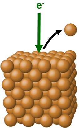
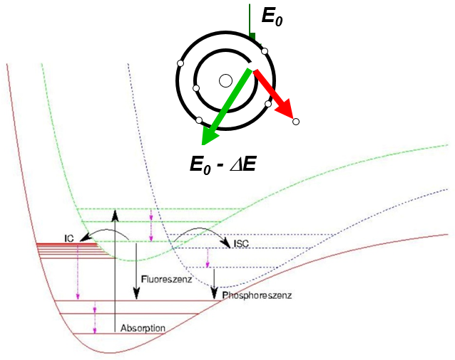
All materials suffer from electron beam damage when illuminated with a high dose in an electron microscope. Two different damage mechanisms are normally considered: 1) knock-on damage (Figure 1), where an incident electron transfers sufficient energy to an atom to displace it from its position; either in the bulk creating an Frenkel pair or sputtering at the surface and 2) radiolysis (Figure 2), where the inelastic interaction between the materials and an incoming electron leads to the formation of an exited state, which then reacts in different ways leading to possible structural changes (Figure 3). Below a certain threshold voltage, no know-on damage is possible, if the electron does not have sufficient kinetic energy to displace the atoms (depending on the element and structure), whereas know-on damage become increasing likely with increasing high-tension. Radiolysis becomes increasingly important at low voltages as the inelastic interaction with the sample is increasing. There is no dose threshold for radiolysis.
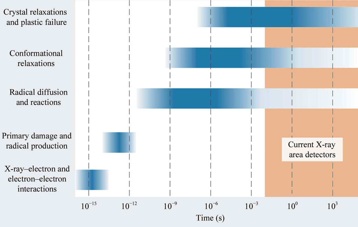
The times scales for the different relaxation processes following the initial excitation in radiolaysis are shown in Figure 3.
|
Figure 1: High-angle ‘elastic’ collision with an atom leading to
|
Figure 2: Inelastic interaction leads to an electronic/vibronic transition to an excited or non-bonding state.
|
Figure 3: Radiolysis time scales from M. Warkentin, et al. Acta Cryst., 2012, D68, 124–133. |
In polymer science, it is well established that electron beam damage, dominated by radiolysis, is one of the major challenges in high-resolution characterization and low-dose imaging techniques are commonly used for nanoscale or atomic level characterization. When working with crystalline materials, the damage is typically assessed by evaluating the changes in intensity of the diffraction peaks to determine structural changes induced by the electron beam. The diffraction pattern is fading ‘from the outside in’ and either the end-point dose (when a diffraction peak disappears completely) or the critical dose (when the diffraction intensity is reduced to 1/e) for a specific diffraction spot are reported as a measure of the beam sensitivity. The beam sensitivity critically depends on high-tension, current density, illuminated area, sample thickness, presence of coatings and temperature, so that one has to be careful by comparing numbers. Nevertheless, a rough comparison is typically possible just considering to the high-tension. The example in Figure 4 shows how the diffraction pattern is fading with increasing dose.
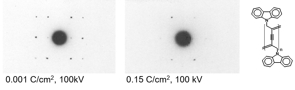
Figure 4: Fading of the diffraction pattern of polyDCHD with increasing dose.
The dependence of the critical/end-point dose on the chemical nature and high-tension can be seen in the extension of the work in L.F. Drummy, J. Yang, D.C. Martin, Ultramicroscopy (2004) 99, 247-256 shown in Figure 5. In general, aliphatic polymers are more beam sensitive than aromatic ones and with increasing high-tension, the stability is increasing.
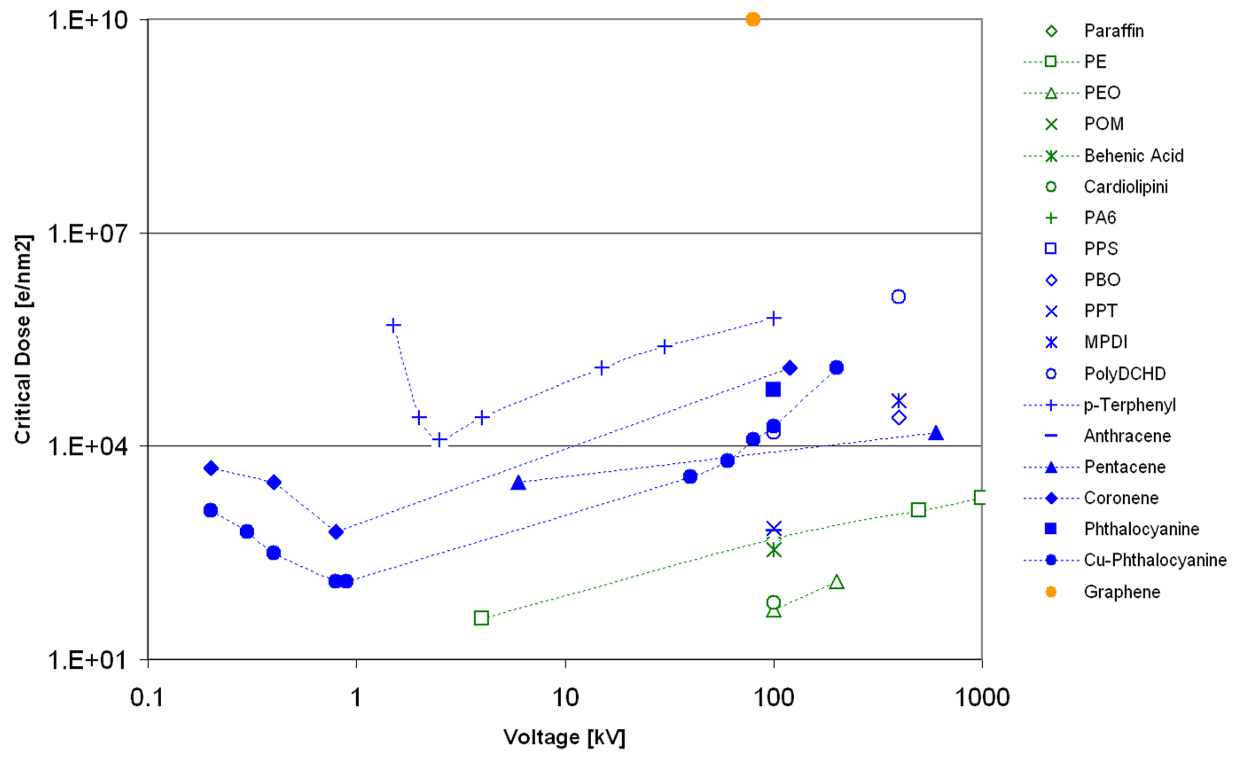
Figure 5: Critical/end-point dose reported in literature for various polymers depending on high-tension.
An interesting alternative to better understand details of the structural changes due to electron beam damage is the use of RDF analysis to follow the damage. As an example, we performed a systematic study of the electron beam induced degradation of P3HT monitoring the structural transitions based on the changes of the short range order: the degradation started with a cleavage of the aliphatic side chains, which enabled a rotation of the polymer chain before it was fragmented at very high dose giving rise to a partially carbonized material.
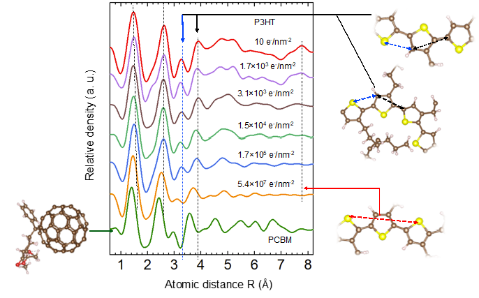
Figure 6: Electron beam induced structural changes in the neat P3HT film measured at 300 keV acceleration voltage with varying dose.
Details are published at
Beam damage is not only critical in polymer research, but also for a large number of other materials. In battery research this has also been recognized for most lithiated compounds, but is not always considered appropriately, especially that already SEM imaging can be detrimental. Figure 7 shows damage induced by the electron beam at different voltages in a LiPON thin film. After applying a dose of 3500 e/nm2 to the central part of the area imaged. The LiPON film is particularly sensitive at voltages between 2-10 kV. The movie with increasing dose at the bottom of the page shows that first changes in the sample are observed already at a dose of 22 e/nm2 at 2 kV and wires start to grow at 430 e/nm2.
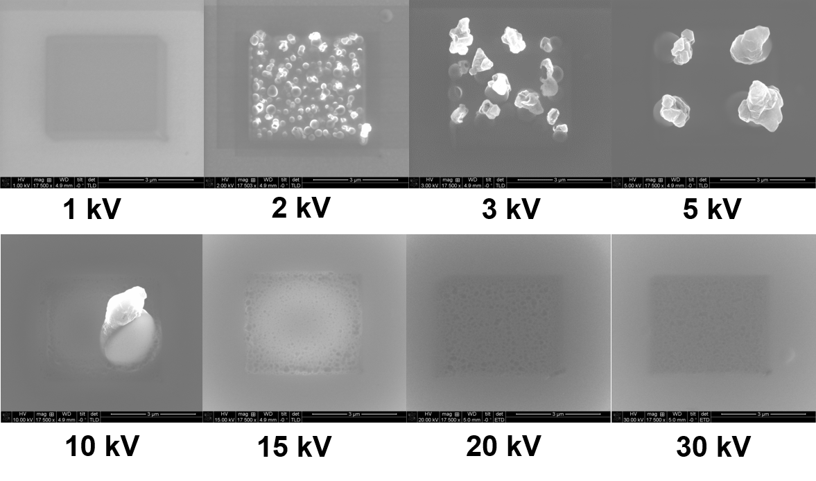
Figure 7: Beam damage induced by SEM image of the central area with a dose of 3500 e/nm2.
(The LiPON films have been prepared in the group of R. Hausbrand, TU Darmstadt).
In case of metal oxides or semiconductor oxides, electron beam damage is typically only considered to be a significant factor for TEM analysis at very high dose. This is partially because the structural changes due to the electron beam are often difficult to identify clearly. However, the electrical properties can change drastically, even at very low dose, for both low and high voltage SEM and TEM. Therefore, we have used the electrical properties measured in-situ as a finger print to identify damage induced by the electron beam in thin films, which is particular important, when electrical properties are critical, e.g. in battery research. Surprisingly, our analysis both of crystalline as well as amorphous metal and semiconductor oxides (SiO2, TiO2, NbOx, BTO) revealed a very high beam sensitivity of the oxides with changes from an insulating to seminconducting and even metallic conductivity already starting at a dose as low as 450 e/nm2 at 300 kV below 10 e/nm2 at 2 kV (Figure 8). Our analysis shows that this damage is due to partial reduction induced by radiolysis of thin films.
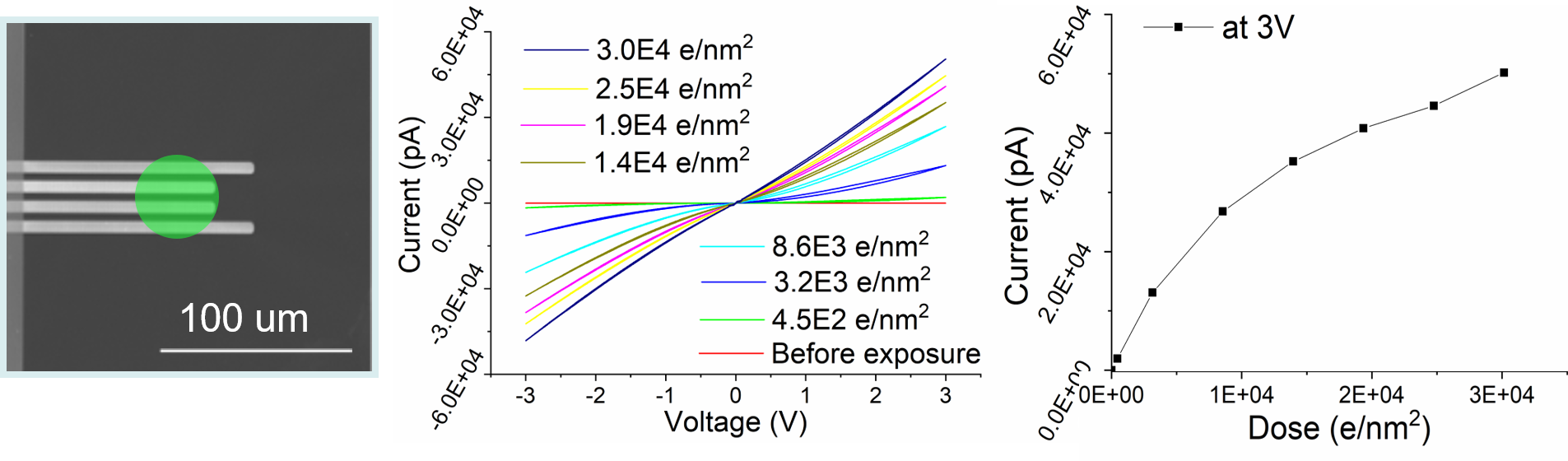
Figure 8: In-situ TEM setup to measure the electrical changes of a thin oxide film deposited on a MEMS electrical chip. The 4 electrodes are visible as bright lines and the position of the electron beam is shown in green. The I/V curves show the changes from an insulating TiO2 film to metallic conductivity with continuous change in conductivity with electron beam exposure.
Details are published at
It is essential to consider these observations for in-situ/operando SEM/TEM investigations. Both, the SEM/FIB sample preparation can lead to significant changes in the structure and the electrical properties as well as the electron beam during the in-situ SEM/TEM measurements, even for materials typically not considered electron beam sensitive.
Closely related, the electronic activation due to inelastic interaction of the sample with the electron beam, can significantly change the chemical reactivity of the investigated material. One example is the significantly changed reactivity seen for graphene flakes with compared to without the electron beam as we have shown in our recent work in Nanoscale Advances. Therefore, kinetic measurements from in-situ SEM/TEM have to be very carefully evaluated.