
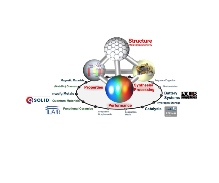
Materials Research
We are using state-of-the-art imaging, spectroscopy and diffraction based electron microscopy techniques, both in-situ and ex-situ, to understand materials and provide a link to simulations. When state-of-the-art techniques do not provide sufficient answers, we tackle research problems by dedicated method developments.
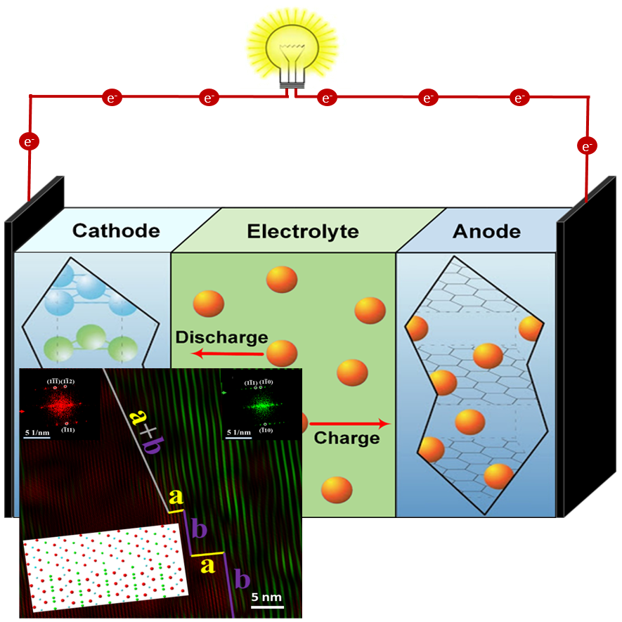
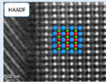
Understanding the structure, chemistry and oxidation state controlling the fundamental processes in batteries and their degradation is challenging, but needed for knowledge based design of new battery systems.
We are addressing structure, composition and morphology from the atomic scale to the micron scale using analytical and 4D-STEM techniques, both in situ and ex situ, to better understand the active sites involved in catalytic reactions, their evolution over time as well as diffusion and flow properties of the overall catalytic system.
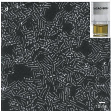
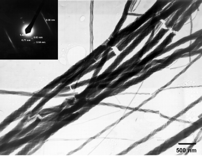
Among various storage strategies, metal hydrides offer high volumetric hydrogen density and favorable reversibility, making them promising candidates for solid-state hydrogen storage.
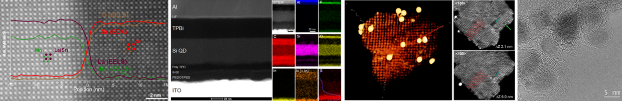
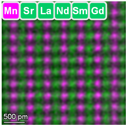
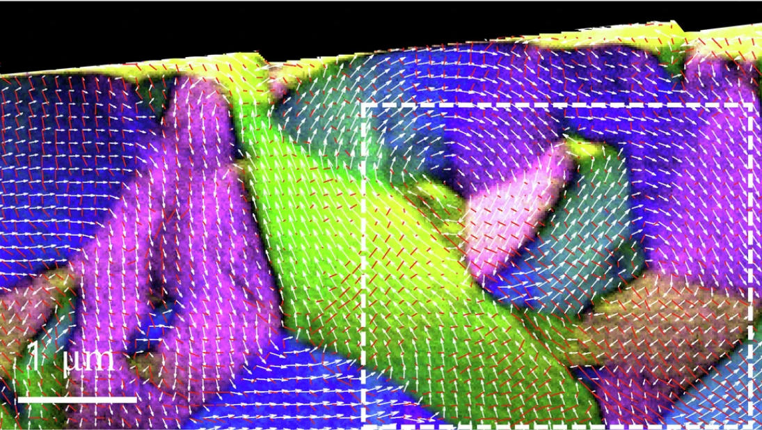
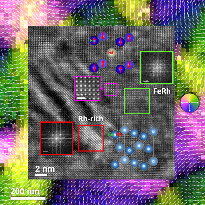
The atomic scale and microstructure together with the local chemistry and electronic structure of a variety of functional ceramics are characterized combining HRTEM, HRSTEM, and STEM-EDX/EELS spectrum imaging. In addition, magnetic and ferroelectric domains can be imaged using 4D-STEM techniques.
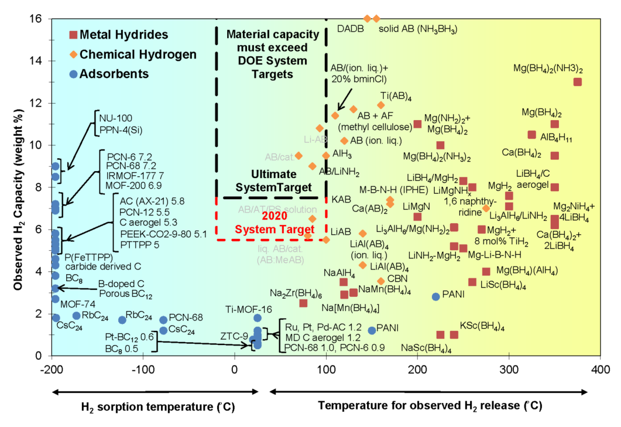
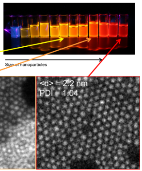
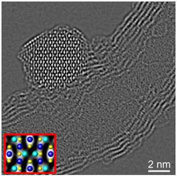
Advanced analytical (S)TEM and 4D-STEM characterization techniques are used to determine the crystal structure, defects and the elemental distribution down to the atomic scale as well as the electronic structure for the different cations.
Furthermore, they promise new energy efficient sensing capabilities. We have investigated new quantum materials using high-resolution imaging and spectroscopy techniques to develop a fundamental understanding of the interplay between real space and electronic structure and their functional properties.
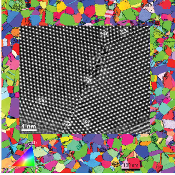
We are employing high-end microscopy approaches to understand how microstructure and defects can be used to tailor mechanical and electrical properties as well as stability of ufg metals.

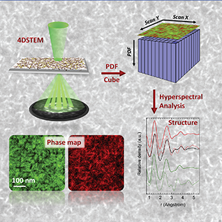
We have developed 4D-STEM based high-sensitivity pair distribution function (PDF), strain and magnetic field mapping as a new approach to simultaneously characterize structural and functional properties of metallic glasses at the nanoscale with high precision.


Microscopy Method Development
We are focusing on four main methodology areas in response to the needs of our collaborations partners, developing approaches for dedicated structural and functional analysis of materials at the atomic, nano- and microscale. A particular focus is on correlated or, ideally, simultaneous structural and functional characterization.
.png)
In situ and operando TEM provides a direct link between structural evolution and materials properties or function and the ability to identify intermediate structures, which cannot be observed ex situ. We are using and optimizing the techniques, combining them with low-dose imaging and various 4D-STEM and spectroscopic techniques for meaningful in situ/operando investigations. Closely related, we are developing identical location FIB/SEM techniques as alternative approach to follow structural evolution using snapshots of the same region at defined states.
link4D-STEM techniques have been shown to be extremely powerful, opening the possibility to (simultaneously) perform high-end structural and functional characterization by combining pair distribution function, crystal orientation and strain mapping together with electric or magnetic field mapping at the nanoscale. In addition, ptychography techniques give access to unprecedented atomic level characterization.
link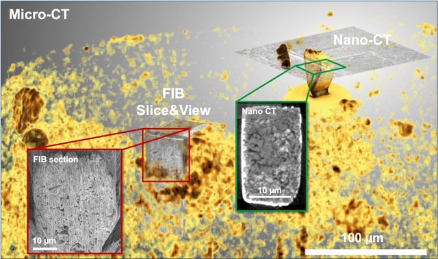
We are establishing correlative characterization workflows that integrate complementary scale bridging imaging techniques such as FIB/SEM, light microscopy, X-ray CT, and TEM into a unified three-dimensional characterization framework.
link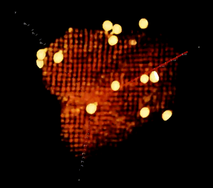
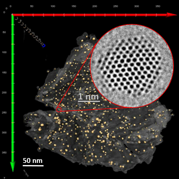
We are developing electron tomography as an approach to quantify the 3D nano and micro structure. In collaborations, we are using these experimental 3D structure as basis for diffusion or flow simulations.
linkSupporting Developments
Using state-of-the-art electron microscopy critically depends on reliable sample preparation, a good understanding of electron beam – matter interactions and research data management to make proper use of the information obtained.
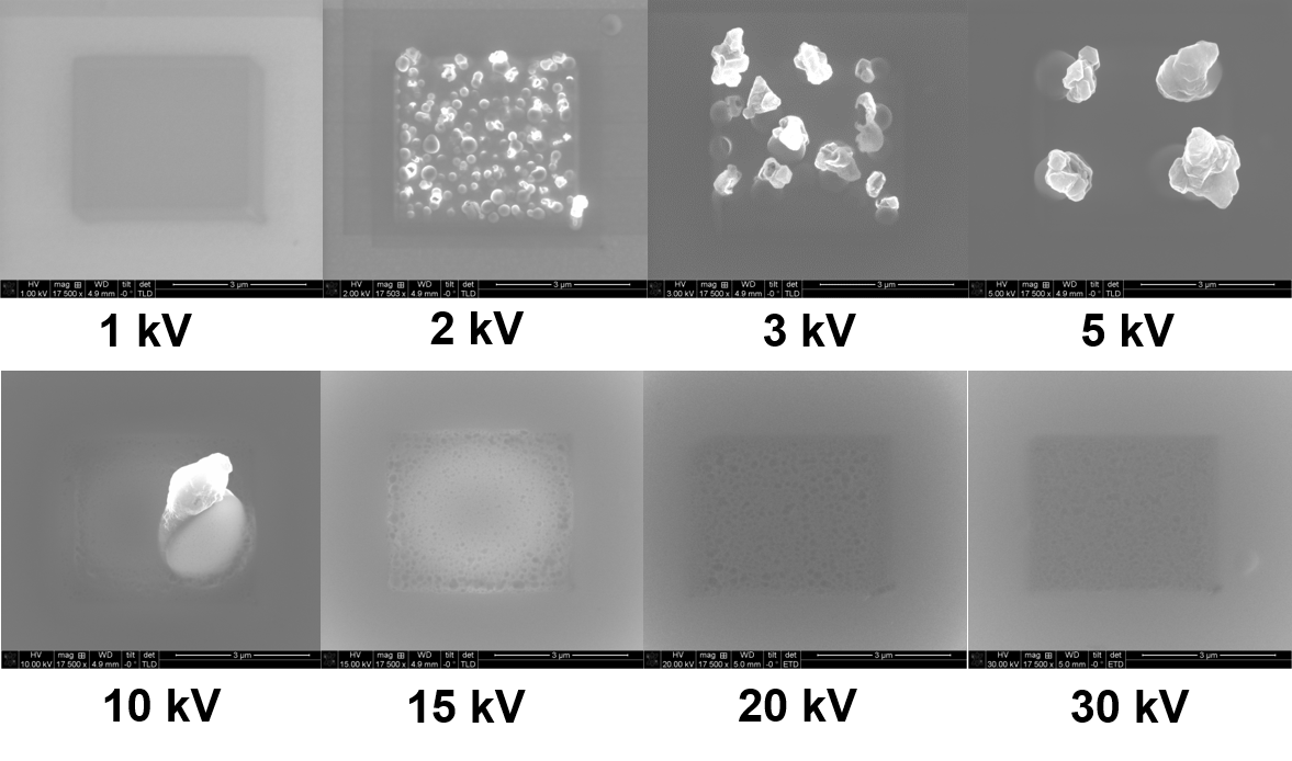
Assessing the effects of the electron beam - matter interaction is important for structural characterization, but even more critical for functional analysis and in in situ/operando microscopy for a meaningful analysis in SEM, FIB and TEM.
link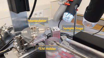
We develop improved handling and preparation methods—especially for air-sensitive and FIB-made samples—to keep TEM specimens as close as possible to their native state.
link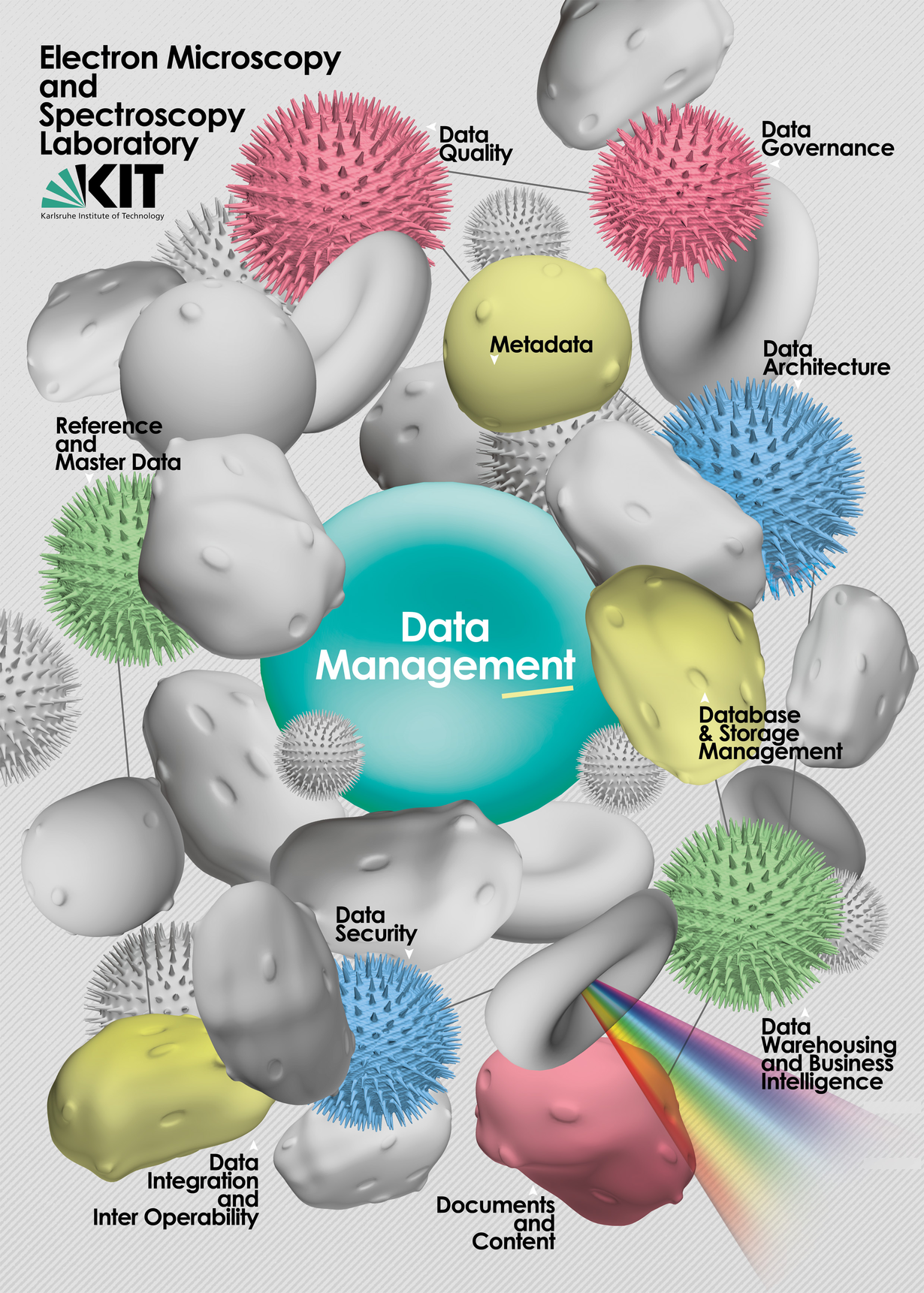
RDA aims to make the research process as reproducible and efficient as possible by providing structured access to information, data & meta-data, enabling best utilization of the experiment results.
link