

Functional Ceramics
Advanced STEM techniques combining HRSTEM-EELS/EDX and 4D-STEM make it possible to visualize the local atomic structure and the corresponding chemistry and the larger scale microstructure using orientation and strain mapping. In combination with 4D-STEM DPC mapping this further enables an analysis of the local electric fields, e.g. around grain boundaries enabling a direction correlation of structural and functional properties to develop a fundamental materials understanding.

Perovskite oxides such as strontium titanate (SrTiO₃) and barium titanate (BaTiO₃) are cornerstone materials in modern electronics and energy technologies. Their unique combination of ionic, electronic, and ferroic functionalities underlies a broad range of applications from capacitors, sensors, and varistors to solid oxide fuel cells and resistive memory devices. What makes these materials particularly fascinating is their tunability: subtle changes in composition, defect chemistry, or local structure can drastically alter their dielectric behavior, conductivity, and even catalytic performance. Understanding how these properties emerge from the atomic structure is therefore a central challenge in materials science.
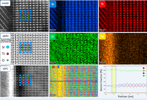
Figure 1. Atomic resolution STEM -HAADF/EDX and STEM-DPC analysis of STO doped with ∼0.8 at % Fe imaged in [110] orientation: An approximately one unit cell wide grain boundary region is visible with Fe enriched to ∼2.3 at% extending slightly into grains. In addition to the Sr at Ti atomc positions, the O colums can also be seen in STEM-DPC.
At the heart of this complexity lie interfaces and grain boundaries, where the structural symmetry breaks and electronic charge redistributes. Dopant atoms tend to segregate at these boundaries, forming so-called space-charge layers that govern ionic transport, local potential barriers, and charge compensation mechanisms. These nanoscale features, though occupying only a small volume fraction, have a decisive influence on the macroscopic performance of perovskite ceramics. For example, they can control grain growth, modify conductivity, and dictate long-term stability during device operation or high-temperature cycling.
Advanced transmission electron microscopy (TEM) now makes it possible to directly visualize these local structures and their chemistry with near-atomic precision. Techniques such as scanning TEM (STEM) combined with electron energy loss spectroscopy (EELS), energy-dispersive X-ray spectroscopy (EDX), and differential phase contrast (DPC) imaging reveal how atoms rearrange, how dopants segregate, and how electronic states evolve across interfaces. When coupled with in-situ heating experiments and quantitative orientation or strain mapping, these approaches uncover how grain boundaries and defect networks change dynamically under realistic conditions.
Electric fields at random grain boundaries
-
Space-charge-layer mapping in polycrystalline BaTiO3 and SrTiO3
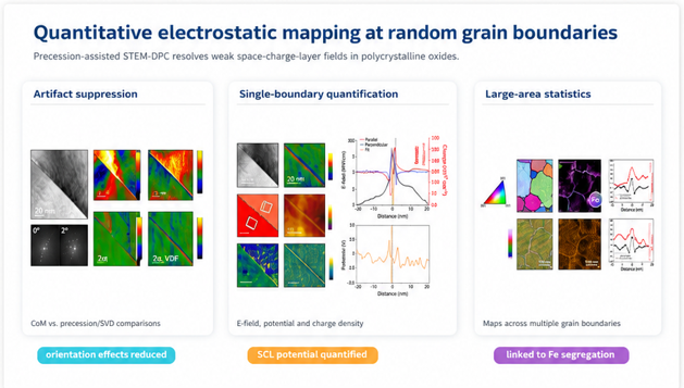
Figure 2. Proposed oxide case-study graphic. The composite highlights artifact reduction, single-boundary quantification and large-area field mapping across multiple grain boundaries.
Space-charge layers at grain boundaries control local electric fields and can influence oxygen-vacancy migration, ionic conductivity and electrical potential barriers in oxide ceramics. These fields are usually weak, local and embedded in complex grain orientation contrast, which makes quantitative DPC analysis challenging.
Using Fe-doped BaTiO3 and SrTiO3 as model systems, the precession-assisted edge/SVD workflow enables grain-boundary-resolved electric-field maps. The field profiles can be integrated to obtain electrostatic-potential maps and differentiated to estimate projected charge-density distributions. In the same regions, 4D-STEM orientation and strain information, together with STEM-EDS elemental maps, can be used to interpret the electrostatic response.
FLAIR - Fermi level engineering applied to oxide electroceramics
Oxide electroceramics power much of modern technology, yet designing them remains largely trial and error, subtle changes in composition or processing can drastically alter their properties for reasons that cannot be predicted. The root cause is the lack of a unifying framework to describe how doping controls material behavior: when a dopant is introduced, its charge can be compensated in multiple competing ways, electronically, ionically, or through valence changes, and which mechanism dominates determines everything from conductivity to piezoelectric performance. FLAIR proposes that the missing unifying parameter is the Fermi level, the electrochemical potential of electrons, which governs the formation energies of all relevant defects and therefore controls which compensation mechanism prevails. In our group by learning to engineer the Fermi level through composition and processing, we gain a rational and predictive approach to ceramic design moving the field from serendipity to science.
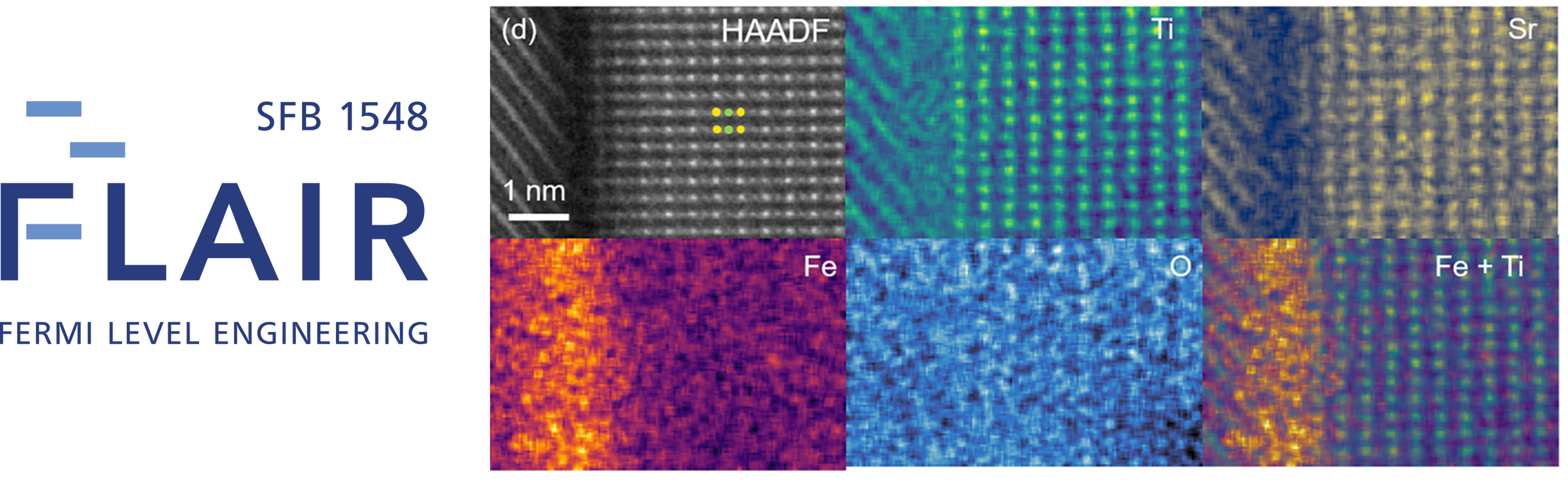
Figure 3. FLAIR application. Low and high-resolution analysis of GB segregation in the 2 % Fe sample. EDS mapping fshowing that Fe segregation is confined within 1–2 unit cells from the grain boundary core.
Through such analyses, researchers aim to establish a direct link between atomic-scale structure, electronic configuration, and macroscopic functionality in perovskite oxides. By correlating structural order, defect chemistry, and Fermi-level variations, we can begin to rationally design materials with tailored electrical, ionic, and thermal behavior. This understanding does not only shed light on the fundamental physics of complex oxides but also informs the development of next-generation functional ceramics for sustainable energy and electronic technologies.
Details to this work have been published at
- Wang, D. et al. Grain boundary segregation in iron doped strontium titanate: From dilute to concentrated solid solutions. Acta Mater., 2024, 273, 119941.