
STEM-DPC and 4D-STEM Field Mapping
Imaging magnetic induction and domains with high spatial resolution is essential to correlate the magnetic properties of materials and devices to their micro- and nanostructure.
- Making electric and magnetic fields visible in functional materials.
Our group develops quantitative scanning transmission electron microscopy differential phase contrast (STEM-DPC) and 4D-STEM methods to map electric and magnetic fields at the nanoscale. By recording a diffraction pattern at each probe position, we track minute momentum changes of the electron beam and transform them into projected field maps that can be directly compared with structural and elemental information.
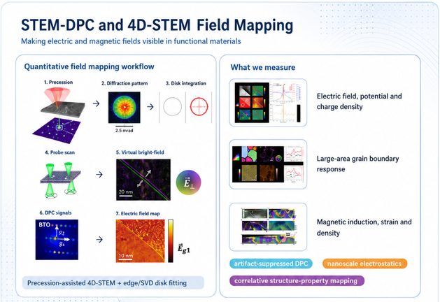
Figure 1. Proposed hero graphic for the STEM-DPC webpage. The composite summarizes precession-assisted 4D-STEM, disk-center fitting and quantitative field mapping.
How the measurement works
- From diffraction shifts to quantitative maps
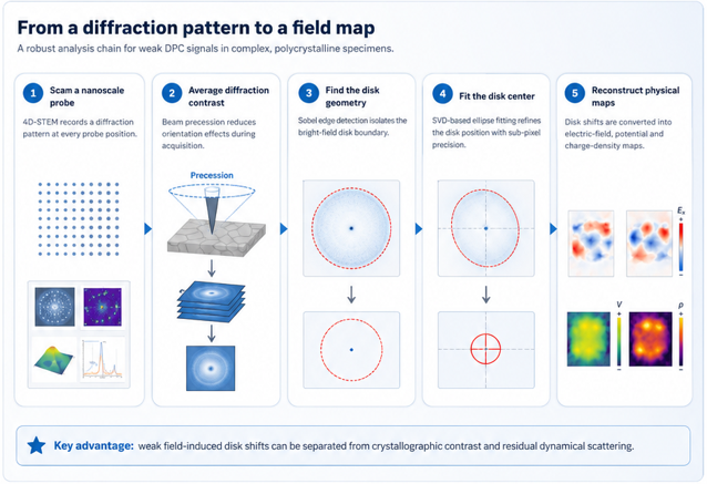
Figure 2. Website-ready workflow graphic: probe scan, 4D diffraction data, precession averaging, Sobel edge detection, SVD disk fitting and field reconstruction.
In STEM-DPC, local electric or magnetic fields deflect the transmitted electron beam. With a pixelated detector, the full diffraction pattern is saved for every probe position, so the analysis can be performed after acquisition and can be tuned to the specimen and the physical quantity of interest.
For weak signals in polycrystalline ceramics, conventional center-of-mass analysis can be biased by orientation contrast, intensity redistribution and dynamical scattering. Our current workflow combines beam precession during acquisition with geometry-based bright-field disk tracking during post-processing. A Sobel edge filter identifies the disk boundary, and SVD-based ellipse fitting extracts the disk center with sub-pixel precision.
- Precession reduces orientation-dependent diffraction contrast while preserving field-induced deflection signals.
- Edge-based fitting focuses on the disk geometry, so asymmetric intensity inside the disk has less influence on the measured shift.
- Vacuum-reference correction and thickness estimation support conversion from projected momentum transfer to quantitative field profiles.
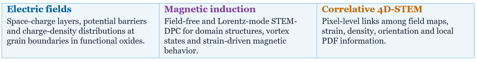
- Complementary 4D-STEM analysis can provide orientation, strain, density and local PDF information from the same experiment.
Application: electric fields at random grain boundaries
-
Space-charge-layer mapping in polycrystalline BaTiO3 and SrTiO3
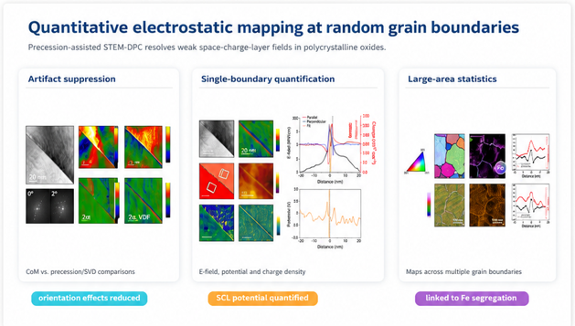
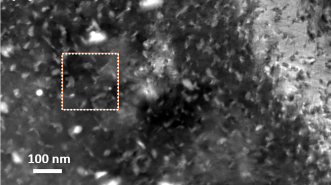
Figure 3. Proposed oxide case-study graphic. The composite highlights artifact reduction, single-boundary quantification and large-area field mapping across multiple grain boundaries.
Space-charge layers at grain boundaries control local electric fields and can influence oxygen-vacancy migration, ionic conductivity and electrical potential barriers in oxide ceramics. These fields are usually weak, local and embedded in complex grain orientation contrast, which makes quantitative DPC analysis challenging.
Using Fe-doped BaTiO3 and SrTiO3 as model systems, the precession-assisted edge/SVD workflow enables grain-boundary-resolved electric-field maps. The field profiles can be integrated to obtain electrostatic-potential maps and differentiated to estimate projected charge-density distributions. In the same regions, 4D-STEM orientation and strain information, together with STEM-EDS elemental maps, can be used to interpret the electrostatic response.
- Random grain boundaries can be screened for local field direction, field strength and electrostatic asymmetry.
- Charge-density maxima can be compared with Fe enrichment and defect-compensation scenarios.
- Atomistic modeling helps separate the extended space-charge-layer signal from mean-inner-potential contributions near the grain-boundary core.
- The method provides a route from local microscopy to materials-level insight into transport barriers and defect redistribution in electroceramics.
_____________________________________________________________________
More details on this work have been published at
-
S. Kang, H. Cho, M. Töllner, A. R. Nelson, Z. Ding, X. Mu, D. Wang, W. Rheinheimer, K. Wang, B.-X. Xu, J. K. Laux, M. Serour, K. Albe, A. Klein and C. Kübel, “Accurate Nanoscale Mapping of Electric Fields across Random Grain Boundaries in Polycrystalline Oxides Using Precession-Assisted 4D-STEM”, manuscript provided for this webpage draft.
- S. Kang, M. Töllner, D. Wang, C. Minnert, K. Durst, A. Caron, R. E. Dunin-Borkowski, J. McCord, C. Kübel and X. Mu, “Large-angle Lorentz Four-dimensional scanning transmission electron microscopy for simultaneous local magnetization, strain and structure mapping”, Nature Communications 16, 1305 (2025). DOI: 10.1038/s41467-025-56521-6.
- R. Witte, R. Kruk, M. E. Gruner, R. A. Brand, D. Wang, S. Schlabach, A. Beck, V. Provenzano, R. Pentcheva, H. Wende and H. Hahn, “Tailoring magnetic frustration in strained epitaxial FeRh films”, Physical Review B 93, 104416 (2016). DOI: 10.1103/PhysRevB.93.104416.
- R. Witte, R. Kruk, A. Molinari, D. Wang, S. Schlabach, R. A. Brand, V. Provenzano and H. Hahn, “Epitaxial strain-engineered self-assembly of magnetic nanostructures in FeRh thin films”, Journal of Physics D: Applied Physics 50, 025007 (2017). DOI: 10.1088/1361-6463/50/2/025007.
-